Dears,
Feedback using TPA3255DDVR to do a 300W stereo power amplifier @4Ω, in the PWM simulation sine wave load test, there is a burnt out IC phenomenon, specifically as follows:
1. 300W, stereo, left and right channel, load 4Ω;
2. No burning problem was found in the test with loudspeaker. With 1KHZ sine wave, the analog signal was about 0.75-1.2V, and IC was burned out during the simulation load test
a. IC is more likely to burn out when the input voltage is 51V than when the input voltage is 45V. According to the customer's feedback, the probability of IC burning out is related to the load time.
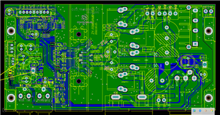
b. See the DEMO on the official website for the PCB Layout
c. Test 2PCS, all of which showed the above phenomenon
d. After the customer adds a fan under the heat sink, it can work normally. The current design heat sink is larger than the DEMO
Attached are the customer's schematic diagram, PCB Layout and test data. Please help to check the case.
Thanks
TPA3255 Test Data.xlsxF0903-schematic.pdfZY-F0903AMP_V1.0.PCB