This thread has been locked.

If you have a related question, please click the "Ask a related question" button in the top right corner. The newly created question will be automatically linked to this question.

TAS2555: TAS2555EVM

Part Number: TAS2555

Hello Ivan,

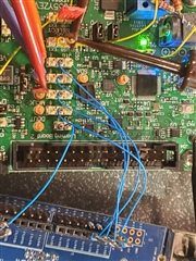
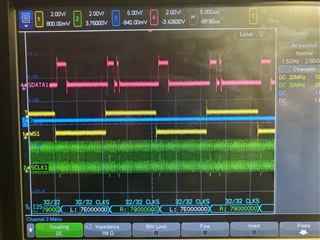
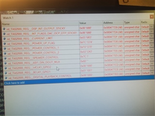
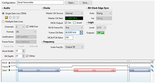
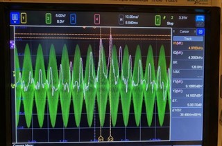
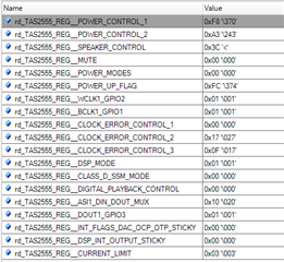
We are having problems driving the TAS2555 with an external master running on a PSOC6 development kit board. Then we found this thread showing that another TI EVM does not allow an external master:

https://e2e.ti.com/support/audio-group/audio/f/audio-forum/621777/tas2521evm-is-is-possible-to-connect-a-master-i2s-to-the-eval-board

Does the TAS2555EVM have a similar restriction for operating with an external master?

Thanks,

Rich

  • Hi Rich,

    TAS2555EVM supports connection with an external host controller, unlike TAS2521EVM.

    You should remove J15, J16, J17 and J18 and connect the external host in its place, as described in User's Guide Section 5.1.2: https://www.ti.com/lit/ug/slou411/slou411.pdf#page=9

    Best regards,
    -Ivan Salazar
    Applications Engineer

  • Hello Ivan,

    Thank you for the reply. We are following the instructions on page 9 of the TAS2555 EVM User Guide. See below.

    We are viewing the I2S from the probes on the TAS2555 EVM test points shown in the picture and the I2S appears clean and error free.

    However with these I2S signals we still do not have an output on the TAS2555 evm (blue line). We are also using J19 and J20 to selectively switch the I2C between the EVM processor and/or out PSoC6 development board processor. See the TAS2555 register configurations below. Note that the Power Up Flags = 0xFC and there are no STICKY error bits being set. Also not that the I2S is driving non-zero signal to both L and R channels.

    The PSoC6 clocking configuration is MCLK = 12.5MHz, BCLK = 3.125MHz, WCLK = 48.828KHz.

    NOTE: also that the TAS2555_REG_WCLK1_GPIO2 is for some reason reporting back 0x00 even though its default value should be 0x01 and we are never writing any other value to it (we do try to write 0x01 back to it, but it still subsequently reads back as 0x00). Is this a smoking gun?

    Rich

  • Rich,

    Do you have an initialization script you can share for review? Did you use PPC3 to generate the script?

    Regarding B0_P1_R0x3e, can you also check what is the status of B0_P1_R0x09? This should set the WCLK to be GPIO2.
    If you use the EVM with on-board controller for both I2S and I2C, along with PPC3, do you have correct operation?

    Best regards,
    -Ivan Salazar
    Applications Engineer

  • Hello Ivan,

    Back in December, you sent the link below to Kurt C. PPC3in a related thread: 

    I reconnected the I2C to the EVM host MCU and pasted that script into the PPC3 I2C monitor and clicked "execute". (NOTE: that our PSoC6 Dev Kit was still actively driving our I2S file.) Once the PPC I2C script download was complete, the audio output immediately began to produce the expected test waveform.

    So it seems like your script works. But now I have some follow up questions, because that "magic" script file is 15000+ lines long and I have no idea how or why it works, and I would have no idea how to reproduce such a script for myself!

    Can you help us understand what goes on in that large script? How it gets generated? And how best to program our embedded TAS2555 devices on production units in the factory?

    Thanks,

    Rich

  • Hi Rich,

    Thanks for the additional information.

    The script I provided was generated using PPC3, as you mentioned. It seems you had access to TAS2555 app but not PPC3, so I just granted access to PPC3 as well.

    Once PPC3 is installed, and TAS2555 plugin within, you can do all the required configuration and testing using mainly the tuning and audio processing as well as Device Control panels.
    When you have your settings all set up, last step is to generate the configuration files. To do this you go to End System Integration panel and follow the steps providing the requested details like:

    • Mode: Tuning (smart amp) mode or ROM (no audio processing) mode
    • Sampling frequency
    • Clock source: MCLK or BCLK
    • Clock frequency: the frequency of your clock source

    This is the step where I selected the settings that most closely matched the provided system description.
    Once the process is completed, the software will generate the required configuration files in different formats:

    • debug_cfg is a format you can use with TI software tools, like PPC3, were you can load a preset of I2C writes into the device.
    • bin file is the one you may use on your end application, which is integrated along with the drivers which you can refer here: https://git.ti.com/cgit/?q=tas2555

    You can find more details on the End System Integration document available online: https://www.ti.com/lit/an/sboa238/sboa238.pdf

    Hopefully this gives a better understanding of the configuration files and how to obtain them. Let me know if there's still any further questions.

    Best regards,
    -Ivan Salazar
    Applications Engineer

  • Hello Ivan,

    Our design is a very simple embedded device with no file system (not android or linux, etc). Precision audio calibration is not a requirement for our device. In fact, the device does not even drive audio or a speaker. We did not anticipate a complex and lengthy audio tuning process. Nor did we anticipate needing an android file system based device to load a large program (such as 48k_3M072_TuningMode_combined_configuration_0_TuningMode_48KHz.cfg) into our device.

    How do we create a BARE BONES .cfg file based on Rom Mode 1 or ROM Mode 2? I see places in PPC3 to set up the parameters but I do not see the method for generating a .cfg file like the one above (only hopefully much, much simpler than that one.

    Thank you for you continued help,

    P.S. Is the any way that TI/You would create a configuration for us? 

    Rich

  • Hi Rich,

    I understand, if you don't really need all the bells and whistles in the digital audio processing ROM mode would be the option to go.
    Please provide the input clocks you're planning to use on your system (BCLK, WCLK and MCLK if used) and I can test a very simple script on my side, then send it to you.

    Best regards,
    -Ivan Salazar
    Applications Engineer

  • The PSoC6 MCU generates all of the clocking configuration is MCLK = 12.5MHz, BCLK = 3.125MHz, WCLK = 48.828KHz.

    Thank You so much!

    Rich

  • Hi Rich,

    Thanks for the data, I'll double check the configuration on my side and share the simple cfg later today or early tomorrow.

    Best regards,
    -Ivan Salazar
    Applications Engineer

  • Hi Rich,

    Attached is the cfg which I've tested with the below input clock settings from AP as I2S master:

    Here's the cfg for ROM mode 2:

    minimalTestROM2.txt
    # Page 0
    w 98 00 00
    # Book 0
    w 98 7f 00
    # Software reset
    w 98 01 01
    # use delay >= 100us
    d 01
    
    # Mute / Powerdown / Reset ends
    
    # PLL begins
    w 98 00 00
    w 98 7f 00
    w 98 00 01
    w 98 73 0f
    w 98 74 0d
    w 98 00 00
    w 98 7f 64
    w 98 1b 01
    w 98 1c 07
    w 98 1d 00
    w 98 1e 00
    w 98 20 07
    w 98 22 08
    w 98 02 10
    w 98 21 04
    w 98 01 08
    w 98 2b 00
    w 98 2c 20
    w 98 1f 20
    w 98 2a 40
    # PLL ends
    
    w 98 00 00
    w 98 7f 00
    w 98 22 02
    
    # Power up 1
    # Page 0
    w 98 00 00
    # Book 0
    w 98 7f 00
    # DSP,PLL, Ndiv , MDAC, MADC  power up
    w 98 04 f8
    
    # Power up 3
    # Page 0
    w 98 00 00
    # Book 0
    w 98 7f 00
    #CLASSD ,Boost power up
    w 98 05 a0
    #CLASSD ,Boost Vsense and Isense power up
    w 98 05 a3
    
    # Unmute Begins
    
    # Delay
    d 01
    
    # Page 0
    w 98 00 00
    # Book 0
    w 98 7f 00
    
    # CLASSD, Isense unmuted
    w 98 07 00
    # Book 100
    w 98 7f 64
    # classD soft unmute
    w 98 07 00
    
    # Unmute Ends

    Best regards,
    -Ivan Salazar
    Applications Engineer

  • Hello Ivan,

    Your ROM MODE 2 config file resolves this issue.

    ONE FOLLOW-UP QUESTION: I will need to tweak a few things in the config, can please you tell me how to get to the "configuration" window that you have screenshotted above? I have searched every PPC3 option but I can't find that configuration window. 

    Thank you,

  • Hi Rich,

    I generated the cfg file using the End System Integration within PPC3 as mentioned before, then I checked which commands could be removed without loosing functionality. What would you need to change?

    The screenshot I shared is from the AP (Audio Precision) test equipment configuration. This is what I used to emulate your system clocks. This is independent from PPC3.

    Best regards,
    -Ivan Salazar
    Applications Engineer

  • Hello Ivan,

    We are seeing some differences in the frequency domain between the TAS2555 amplifier audio output from that of the "legacy" audio output which was based on an NXP TFA9879 Amp. What we’re trying to solve is to get the frequency content of the prototype output waveform to more closely match the frequency content of the legacy products waveform.

    The Legacy product waveform (in the photo below) shows how there are 2 dominant frequencies (purple spikes with vertical cursors through them) at ~3.910kHz and ~4.034kHz.

    The TAS2555 based prototype's waveform (photo below) shows the 2 most dominant frequencies are close to meeting the product requirement but you can see there are many extra prominent frequency spikes in purple compared to the legacy waveform. 

    We are trying to understand the origin of the more prominent side bands with the TAS2555 and how to minimized them?

    Thank you for you continued assistance,

    Rich


  • Hi Rich,

    Perhaps you have to enable the spread spectrum mode for the output Class-D switching scheme.
    Could you please try by adding a command in the init script to enable bit 0 from B0_P0_R40?:

    Spread spectrum mode is basically changing the output switching center frequency to be changing with a small variation, instead of a fixed frequency which usually reduces the harmonics associated with the square-wave switching itself.

    Best regards,
    -Ivan Salazar
    Applications Engineer

  • Spread spectrum was not enabled. But we found the solution on a web article covering double side band supressed carrier (DSB-SC) signals. Our table only had a half-wave. We needed to increase the table to include the full wave data.

    Thank you, 

  • Hello Ivan,

    This is a new (but related) question...

    We have a different prototype PCB (intended to be identical to the previous PCB discussed in this thread) using the TAS2555. However this new prototype has a schematic/layout error. The I2S data from the MCU is routed into the TAS2555 DOUT1 pin and, unfortunately, the TAS2555 DIN1 pin is NC so that there is no "easy" way to cut and jump a board level fix without removing the TAS2555 BGA.

    Reviewing the TAS2555 datasheet, it seems plausible that the part can be re-configured to accept I2S data input on the DOUT1_GPIO3 pin if the following two TAS2555 registers are overwritten as shown below: 

    /*0-1-0x3f*/
    Amp2555_i2cRegWrite(TAS2555_REG__DOUT1_GPIO3, 0x01);

    /*0-1-0x0c*/
    Amp2555_i2cRegWrite(TAS2555_REG__ASI1_DIN_DOUT_MUX, 0x10);

    If we add these changes to the configuration, the TAS 2555 is reporting No STICKY Errors, POWER UP FLAGS == 0xfc, and all the other TS2555 registers read appropriate values back. However, we still do not see and Class-D audio output (SPK_P and SPK_M are flatlined).

    Can you confirm if the commands above would (or would not) result in the TAS2555 accepting the I2S data input on its DOUT1 pin? And if I made some error in the setting updates above, can you tell me if there is some other setting that would accomplish the desired re-route?

    Thank you,

  • Hi Rich,

    I assume you already read back these registers 0x0c and 0x3f after playback attempt, and still receiving the modified values correct?
    The proposed changes seem feasible to me, but I don't think this is something we've been testing before. I'll give it a try tomorrow or Tuesday next week and will let you know what I can learn from it.

    Best regards,
    -Ivan Salazar
    Applications Engineer

  • We have a debugging area in our code that reads back the values of the TAS2555 registers. When we enable a breakpoint we can view the register values. We have confirmed that registers 0x0c and 0x3f can retain the modified settings of 0x10 and 0x01 respectively. Occasionally, we have noticed that the 0x3f register will not accept the 0x01 setting, but usually it does. I am not sure if, perhaps, the order of the writes may cause the 0x3f register to refuse it's new value. I could test that.

    But I would greatly appreciate if you could try this rerouting yourself to confirm if it will work.

    Thanks,

  • Hello Ivan,

    From the datasheet, ROM MODE 2 activates the DSP and V/I Sense and directs data to the DOUT pin. Do you think the DOUT_GPIO3 register may reject a setting override command if the DOUT function is already allocated by the active DSP?

    Would ROM MODE 1 be more appropriate?

    Thanks,

  • Hi Rich,

    Today is a TI Holiday. Your question will be seen by Ivan tomorrow and you should expect a reply within 48 hours from now.

    Please wait to reply unless we have failed to respond to you in a timely manner.

    Thank you for your patience,

    Jeff McPherson

  • Hi Rich,

    I'll give this a try either today or tomorrow, but I agree ROM mode 1 may be a good idea if IV-sense is not being used anyways.
    In addition to that I'll check if setting reg 0x0c bits 0-1 to ASI1_DIN loopback could help.

    I'll keep you posted on any updates.

    Best regards,
    -Ivan Salazar
    Applications Engineer

  • Hi Rich,

    I just setup the EVM and give this a try:

    • Good news is that I'm able to configure the device to use DOUT-GPIO3 as DIN instead.
    • Maybe not so good news is that I'm doing what I think you're doing; it even worked OK in ROM mode 1 or 2, also the command sequence for 0x0c and 0x3f doesn't seem to matter. Perhaps there's some difference we're not considering.

    I used the same script I shared before in this same thread, and add a few more lines to configure registers 0x0c and 0x3f, I also modified DSP mode to ROM mode 1 just in case. Could you please try this or compare to your script?

    DINtoDOUTTestROM1.txt
    # Page 0
    w 98 00 00
    # Book 0
    w 98 7f 00
    # Software reset
    w 98 01 01
    # use delay >= 100us
    d 01
    
    # Mute / Powerdown / Reset ends
    
    # PLL begins
    w 98 00 00
    w 98 7f 00
    w 98 00 01
    w 98 73 0f
    w 98 74 0d
    w 98 00 00
    w 98 7f 64
    w 98 1b 01
    w 98 1c 07
    w 98 1d 00
    w 98 1e 00
    w 98 20 07
    w 98 22 08
    w 98 02 10
    w 98 21 04
    w 98 01 08
    w 98 2b 00
    w 98 2c 20
    w 98 1f 20
    w 98 2a 40
    # PLL ends
    
    w 98 00 00
    w 98 7f 00
    # DSP ROM Mode 1
    w 98 22 01
    
    w 98 00 00
    w 98 7f 00
    w 98 00 01
    # GPIO3 = Input mode
    w 98 3f 01
    # ASI1_DIN = GPIO3
    w 98 0c 10
    
    # Power up 1
    # Page 0
    w 98 00 00
    # Book 0
    w 98 7f 00
    # DSP,PLL, Ndiv , MDAC, MADC  power up
    w 98 04 f8
    
    # Power up 3
    # Page 0
    w 98 00 00
    # Book 0
    w 98 7f 00
    #CLASSD ,Boost power up
    w 98 05 a0
    #CLASSD ,Boost Vsense and Isense power up
    w 98 05 a3
    
    # Unmute Begins
    
    # Delay
    d 01
    
    # Page 0
    w 98 00 00
    # Book 0
    w 98 7f 00
    
    # CLASSD, Isense unmuted
    w 98 07 00
    # Book 100
    w 98 7f 64
    # classD soft unmute
    w 98 07 00
    
    # Unmute Ends
    
    
    w 98 00 00
    w 98 7f 00
    w 98 00 01
    r 98 0c 01
    r 98 3f 01

    Could there be any other difference in hardware? You can share your schematic and layout files for review.

    Best regards,
    -Ivan Salazar
    Applications Engineer

  • Hi Ivan

    I am the hardware engineer working with Rich on this.  I tested your ROM Mode 1 script but I still don't see any PWM outputs.  I am able to read these register values back using PSoC Creator.  Does anything look incorrect to you?  I included our schematic circuit too.

    How are you able to confirm your ROM Mode 1 (or 2) script works with DOUT-GPIO3 as DIN?  Are you able to swap input connections to a TAS2555 EVM and verify the output looks (or sounds) good?

     TAS2555_Schematic.pdf

  • Hi Brad,

    I'm able to connect the data signal from the audio source into DOUT pin, if I connect to DIN there is no audio with this new script. I just tested functionality by checking audio is being output and is same as when using the original script with DIN.

    Can you share scope captures of your input clocks just to double check these are OK?
    Also can you confirm you're following the same command sequence as in the script? I assume you have to parse the script into whatever syntax your system is using correct? I haven't tried other sequence combinations but the one I shared works at least on the EVM.

    Best regards,
    -Ivan Salazar
    Applications Engineer

  • Hello Ivan,

    Thank you for confirming that the DIN/DOUT rerouting worked for you. 

    I have a few responses below, but Brad may have additional comments to add.

    I used the same parser that I used for the previous two config files you sent in this thread. The ROM 1 code that it generated is shown below.

    I2C_code.txt
    // Page 0
    Amp2555_i2cRegWrite(0x00, 0x00);
    // Book 0
    Amp2555_i2cRegWrite(0x7f, 0x00);
    // Software reset
    Amp2555_i2cRegWrite(0x01, 0x01);
    // use delay >= 100us
    BlockingDelayMs(0x01);
    // Mute / Powerdown / Reset ends
    // PLL begins
    Amp2555_i2cRegWrite(0x00, 0x00);
    Amp2555_i2cRegWrite(0x7f, 0x00);
    Amp2555_i2cRegWrite(0x00, 0x01);
    Amp2555_i2cRegWrite(0x73, 0x0f);
    Amp2555_i2cRegWrite(0x74, 0x0d);
    Amp2555_i2cRegWrite(0x00, 0x00);
    Amp2555_i2cRegWrite(0x7f, 0x64);
    Amp2555_i2cRegWrite(0x1b, 0x01);
    Amp2555_i2cRegWrite(0x1c, 0x07);
    Amp2555_i2cRegWrite(0x1d, 0x00);
    Amp2555_i2cRegWrite(0x1e, 0x00);
    Amp2555_i2cRegWrite(0x20, 0x07);
    Amp2555_i2cRegWrite(0x22, 0x08);
    Amp2555_i2cRegWrite(0x02, 0x10);
    Amp2555_i2cRegWrite(0x21, 0x04);
    Amp2555_i2cRegWrite(0x01, 0x08);
    Amp2555_i2cRegWrite(0x2b, 0x00);
    Amp2555_i2cRegWrite(0x2c, 0x20);
    Amp2555_i2cRegWrite(0x1f, 0x20);
    Amp2555_i2cRegWrite(0x2a, 0x40);
    // PLL ends
    Amp2555_i2cRegWrite(0x00, 0x00);
    Amp2555_i2cRegWrite(0x7f, 0x00);
    // DSP ROM Mode 1
    Amp2555_i2cRegWrite(0x22, 0x01);
    Amp2555_i2cRegWrite(0x00, 0x00);
    Amp2555_i2cRegWrite(0x7f, 0x00);
    Amp2555_i2cRegWrite(0x00, 0x01);
    // GPIO3 = Input mode
    Amp2555_i2cRegWrite(0x3f, 0x01);
    // ASI1_DIN = GPIO3
    Amp2555_i2cRegWrite(0x0c, 0x10);
    // Power up 1
    // Page 0
    Amp2555_i2cRegWrite(0x00, 0x00);
    // Book 0
    Amp2555_i2cRegWrite(0x7f, 0x00);
    // DSP,PLL, Ndiv , MDAC, MADC  power up
    Amp2555_i2cRegWrite(0x04, 0xf8);
    // Power up 3
    // Page 0
    Amp2555_i2cRegWrite(0x00, 0x00);
    // Book 0
    Amp2555_i2cRegWrite(0x7f, 0x00);
    // LASSD ,Boost power up
    Amp2555_i2cRegWrite(0x05, 0xa0);
    // LASSD ,Boost Vsense and Isense power up
    Amp2555_i2cRegWrite(0x05, 0xa3);
    // Unmute Begins
    // Delay
    BlockingDelayMs(0x01);
    // Page 0
    Amp2555_i2cRegWrite(0x00, 0x00);
    // Book 0
    Amp2555_i2cRegWrite(0x7f, 0x00);
    // CLASSD, Isense unmuted
    Amp2555_i2cRegWrite(0x07, 0x00);
    // Book 100
    Amp2555_i2cRegWrite(0x7f, 0x64);
    // classD soft unmute
    Amp2555_i2cRegWrite(0x07, 0x00);
    // Unmute Ends
    Amp2555_i2cRegWrite(0x00, 0x00);
    Amp2555_i2cRegWrite(0x7f, 0x00);
    

    I believe the clocking is not the problem because Brad had the ROM 1 code above successfully working on a correctly laid out board (and with the two DIN/DOUT re-routing commands commented out). 

    Rich

  • Hi Rich, Brad,

    Thanks for the further details, the script seems OK and you could also confirm the previous script parsed with the same method works.

    Is there any other change on the hardware side? Did you have the same output filter components connected to SPK_P and SPK_M?

    Best regards,
    -Ivan Salazar
    Applications Engineer

  • Hi Ivan

    There are no intended changes on the hardware side.  The schematics are the same.  The components are the same.  The PCB layout is as close to the same as possible (but different board shape so some routes are minorly different).  Yes, parsing of the scripts works for the board where we can physically rework and connect DOUT to DIN (and comment out the DIN/DOUT pin swap register write commands).  

    What puzzles me is we get no PWM outputs on the board where we try the DIN/DOUT pin swap. 

    Can you think of any scenarios where the TAS2555 can receive valid I2S inputs, have valid power rails, have valid I2C register configuration but the PWM outputs are disabled (either through some other configuration or because of an error condition that is not reported in a published register location)?  Are there some unpublished register locations we can read to gain more insight?  Or maybe there are registers that would inform if the I2S input data is not passing through to the output stage or the internal oscillator isn't working for us.  

    Do you think power sequencing can cause the PWM outputs to lock up or be disabled?  We noticed previously that the EVM doesn't follow the power rail sequencing guidelines and I don't think we follow them either but can that matter?  The EVM seems to work without following the guidelines.  

  • Hi Brad,

    I'll double check if there could be a noise gate feature or similar enabled by default that could halt the PWM from switching when there is no valid data input.
    This is an old device so I don't have all this fresh in my memory, but can check it on the bench and let you know tomorrow morning.

    Best regards,
    -Ivan Salazar
    Applications Engineer

  • Hi Brad,

    Not sure if you identified the cause of this but just closing up on this thread, I verified there is not a noise gate in this device, so the outputs should be switching with a low duty cycle when idle.
    There may be some reason that the device is not actually being enabled or being automatically disabled by some event, you may use a scope and trigger on either edge of the output PWM to see if it switches at least a bit and then it stops or not switching at all.

    Best regards,
    -Ivan Salazar
    Applications Engineer