This thread has been locked.

If you have a related question, please click the "Ask a related question" button in the top right corner. The newly created question will be automatically linked to this question.

PCM1821EVM: Audio forum

Part Number: PCM1821EVM
Other Parts Discussed in Thread: PCM1821

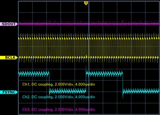
I'm having trouble getting any output from the SDOUT pin of my PCM1821EVM.  I have the jumpers inserted according to Figure 4-2 for Onboard Microphones.  I have the J5 jumper selecting 3.3V for IOVDD, J4 selecting AVDD for MPWR. J9 & J10 inserted, passing 3.3V to AVDD and IOVDD, I have the configuration jumpers all set to 0 (J12, J17, J18, and J20) for slave mode.  I believe my BCLK and FSYNC signals are good, as shown in the attached waveform capture.  However, I don't ever see any non-zero data on SDOUT.  In the attached waveform I'm probing at the green testpoints for FSYNC, BCLK, and SDOUT.  I've confirmed that there is at least some signal on IN1P and IN1M, so I don't believe the failure to get non-zero SDOUT data is due to lack of signal.  Suggestions?  Thanks in advance.

  • Hey Chris, 

    Thanks for bringing this to our attention. These would be looked into within the next 24-48 business hours. 

    Best regards, 

    Ore. 

  • It turns out that the number of BCLKs per FSYNC was not sufficient.  The above shows 16 BCLKs per FSYNC phase.  The PCM1821 looks to need at least 32 BCLKs per phase of FSYNC, or at least 64x FSYNC frequency.

  • Hey Chris,

    It's advisable to follow Table 8-3 and Table 8-4 as a guide to determine the BCLK and FSYNC ratios required for your application. 

    Best regards,

    Ore.

  • I looked at those tables, but they show values below 32 BCLKs per FSYNC phase, which may be appropriate for the PCM mode, but don't seem valid for the I2S mode.  Is that correct?

  • The audio serial interface options are either TDM or I2S modes. 

    Allow 12-24hrs to figure out how to get the SDOUT working on your end. 

  • Hey Chris,

    I powered the PCM1821 on my side with your configuration and it worked. If you follow the onboard mic diagram in the user's guide and have shunts over j9,j10, j5(selecting 3.3V), j20,j13,j17 & j18 connected low, there should be a reading in SDOUT. also a correction, j12 isn't going low, it should be connected with a shunt to allow mic output to the adc.

    Attached are the are the frame clk and bit clk configurations and SDOUT reading.

    Hope this helps. 

    Best regards,

    Ore.

  • I had a typographical error in my original description.  I indicated that I had J12 a configuration jumper set to 0, but it should have been written J13 (MSZ) being configured as 0.  I did have J12 inserted to bring the mic input to the PCM1821.

    It looks like you have BCLK rate at 64x the frame clock.  My oscilloscope diagram showed 16 BCLKs for each level of FSYNC.  I think that's invalid for I2S mode.  Is that incorrect?

    I don't think slave mode uses MCLK, but you're configuration above seems to use MCLK.  Am I missing something?

  • The adc had an SDOUT signal operating with 32BCLK per channel. If the ADC is in slave mode, the external device in master mode provides the MCLK. 

    My configuration shows the external device's MCLK. Here are the oscilloscope readings. FCLK, BCLK, and SDOUT.

    Hope this helps.