Hello,
we designed in the PCM1840 on a board. There are 5 ADCs, 1 x as master and 4 x as slave. After a few adjustments, these work well and the processing in the FPGA also works very well.
Our question now is whether the following sequences are okay or whether adjustments are still necessary for stable operation.
Info: AVDD = IOVDD with the same voltage level 3,3 V
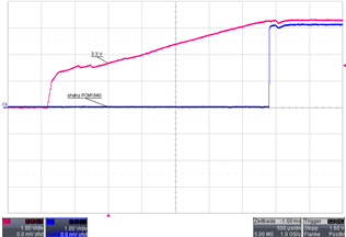
1. PowerUp behaviour:

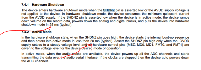
Information from the data sheet: Shdnz must still be kept 100 us low after the 3.3 V supply is stable.
But at what voltage level the 3.3 V considered as stable?
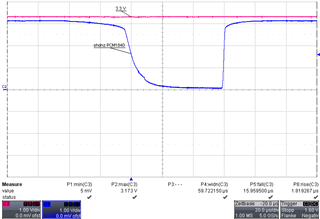
2. Reset during normal operation (AVDD and IOVDD are stable with 3,3 V voltage level):

We did not found a minimum time for an active reset (shdnz = low) in the datasheet. Is this time sufficient to reset the ADC or what is the minimum time on shdnz to reset the ADCs?
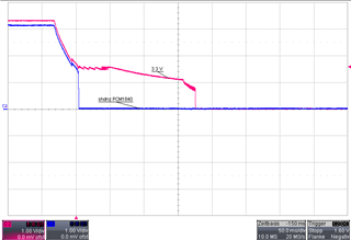
3. PowerDown:

If the power supply run down, we can't pull the shutdown pin (SHDNZ) low (shutdown is active) 10 ms or any time before AVDD and IOVDD run down under the minimum recommended voltage of 3.0 V.
When this voltage drops, the ADC data is no longer processed. This means that it does not matter what the ADC delivers on its data lines.
After this sequence it starts later like in point "1. PowerUp behaviour"
Is this behaviour okay?
Our question now is are thease sequences 1 , 2 and 3 are okay or whether adjustments are still necessary for stable operation in the field by our customers?
We look forward to your feedback with more information.
Thank you and best regard,


