Part Number: TAS2780
Hi,
I have two systems using the TAS2780, one development setup (using the TAS2780EVM) that is working fine and a PCB with an integrated TAS2780 which I cannot get to work.
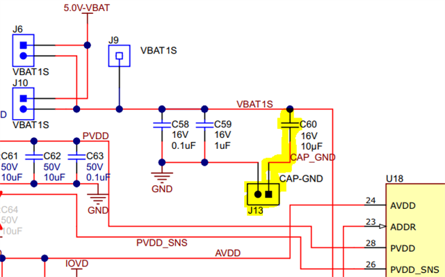
The dev system has 12V on PVDD, the integrated setup has 20V on PVDD. VBAT1S has no external connection and should be generated internally. I adapted the jumper configuration on the TAS2780EVM to match the integrated setup.
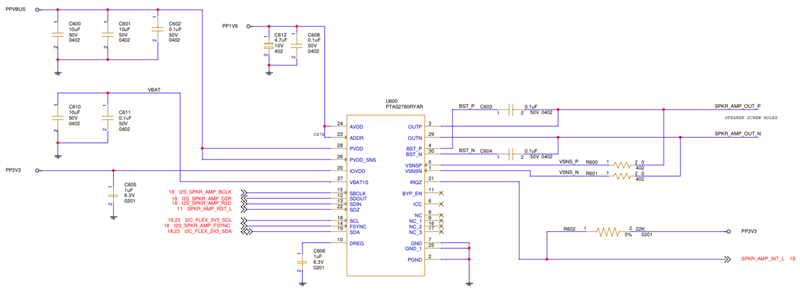
I wrote some python code to set up power mode 2 and set the device in load diagnostic and in diagnostic generator mode and I can hear the beep on both systems.
After loading the kernel driver (which just resets and sets up power mode 2), I can play sounds on the dev system but on the integrated system there is no sound output.
Using the python script, I'm printing the content of the INT_LIVE and the INT_LTCH registers and I see slight differences between the two systems but I'm having difficulties interpreting them.
Here is the script I'm using: https://gitlab.com/-/snippets/2508725
I'm attaching the output of the script from both systems.
Can you help finding the problem?
Also, is the load calculation correct in the script? The spec sheet says the value is in Ohms but it looks more like Milliohms, the connected speaker is 8Ohm.
Is there any other diagnostics that I can run?
Thanks!
Stephan
# Dev system (working fine)

***** Resetting
wrote reg 0x00 value 0x00, read back 0x00
wrote reg 0x7f value 0x00, read back 0x00
wrote reg 0x01 value 0x01, read back 0x00
read reg 0x02 (MODE_CTRL): 0x1a
read reg 0x03 (CHNL_0): 0x28
read reg 0x04 (DC_BLK0): 0x21
read reg 0x42 (INT_LIVE0): 0x00
read reg 0x43 (INT_LIVE1): 0x00
read reg 0x44 (INT_LIVE1_0): 0x00
read reg 0x47 (INT_LIVE2): 0x00
read reg 0x48 (INT_LIVE3): 0x00
read reg 0x49 (INT_LTCH0): 0x00
read reg 0x4a (INT_LTCH1): 0x00
read reg 0x4b (INT_LTCH1_0): 0x00
read reg 0x4f (INT_LTCH2): 0x00
read reg 0x50 (INT_LTCH3): 0x00
read reg 0x51 (INT_LTCH4): 0x00
read reg 0x52 (VBAT_MSB): 0x00
read reg 0x53 (VBAT_LSB): 0x00
VBAT1S Voltage: 0.000V
read reg 0x54 (PVDD_MSB): 0x00
read reg 0x55 (PVDD_LSB): 0x00
PVDD Voltage: 0.000V
wrote reg 0x00 value 0x04, read back 0x04
wrote reg 0x00 value 0x00, read back 0x00
Load: 12607.650000000001 Ohm
***** Initializing power mode 2
wrote reg 0x0e value 0x44, read back 0x44
wrote reg 0x0f value 0x40, read back 0x40
wrote reg 0x00 value 0x01, read back 0x01
wrote reg 0x17 value 0xc0, read back 0xc0
wrote reg 0x19 value 0x00, read back 0x00
wrote reg 0x21 value 0x00, read back 0x00
wrote reg 0x35 value 0x74, read back 0x74
wrote reg 0x00 value 0xfd, read back 0xfd
wrote reg 0x0d value 0x0d, read back 0x0d
wrote reg 0x3e value 0x4a, read back 0x4a
wrote reg 0x0d value 0x00, read back 0x00
wrote reg 0x00 value 0x00, read back 0x00
wrote reg 0x03 value 0xe8, read back 0xe8
wrote reg 0x04 value 0xa1, read back 0xa1
wrote reg 0x71 value 0x0e, read back 0x0e
read reg 0x02 (MODE_CTRL): 0x1a
read reg 0x03 (CHNL_0): 0xe8
read reg 0x04 (DC_BLK0): 0xa1
read reg 0x42 (INT_LIVE0): 0x00
read reg 0x43 (INT_LIVE1): 0x00
read reg 0x44 (INT_LIVE1_0): 0x00
read reg 0x47 (INT_LIVE2): 0x00
read reg 0x48 (INT_LIVE3): 0x00
read reg 0x49 (INT_LTCH0): 0x00
read reg 0x4a (INT_LTCH1): 0x00
read reg 0x4b (INT_LTCH1_0): 0x00
read reg 0x4f (INT_LTCH2): 0x00
read reg 0x50 (INT_LTCH3): 0x00
read reg 0x51 (INT_LTCH4): 0x00
read reg 0x52 (VBAT_MSB): 0x00
read reg 0x53 (VBAT_LSB): 0x00
VBAT1S Voltage: 0.000V
read reg 0x54 (PVDD_MSB): 0x00
read reg 0x55 (PVDD_LSB): 0x00
PVDD Voltage: 0.000V
wrote reg 0x00 value 0x04, read back 0x04
wrote reg 0x00 value 0x00, read back 0x00
Load: 12607.650000000001 Ohm
***** Running load diagnostic
wrote reg 0x02 value 0x13, read back 0x13
read reg 0x02 (MODE_CTRL): 0x13
read reg 0x03 (CHNL_0): 0xe8
read reg 0x04 (DC_BLK0): 0xa1
read reg 0x42 (INT_LIVE0): 0x00
read reg 0x43 (INT_LIVE1): 0x02
read reg 0x44 (INT_LIVE1_0): 0x19
read reg 0x47 (INT_LIVE2): 0x00
read reg 0x48 (INT_LIVE3): 0x00
read reg 0x49 (INT_LTCH0): 0x00
read reg 0x4a (INT_LTCH1): 0x02
read reg 0x4b (INT_LTCH1_0): 0x19
read reg 0x4f (INT_LTCH2): 0x00
read reg 0x50 (INT_LTCH3): 0x00
read reg 0x51 (INT_LTCH4): 0x06
read reg 0x52 (VBAT_MSB): 0x26
read reg 0x53 (VBAT_LSB): 0x0d
VBAT1S Voltage: 4.750V
read reg 0x54 (PVDD_MSB): 0x31
read reg 0x55 (PVDD_LSB): 0x8d
PVDD Voltage: 12.375V
wrote reg 0x00 value 0x04, read back 0x04
wrote reg 0x00 value 0x00, read back 0x00
Load: 9675.9 Ohm
***** Playing diagnostic tone
wrote reg 0x02 value 0x1d, read back 0x1d
read reg 0x02 (MODE_CTRL): 0x1d
read reg 0x03 (CHNL_0): 0xe8
read reg 0x04 (DC_BLK0): 0xa1
read reg 0x42 (INT_LIVE0): 0x00
read reg 0x43 (INT_LIVE1): 0x02
read reg 0x44 (INT_LIVE1_0): 0x11
read reg 0x47 (INT_LIVE2): 0x00
read reg 0x48 (INT_LIVE3): 0x00
read reg 0x49 (INT_LTCH0): 0x04
read reg 0x4a (INT_LTCH1): 0x22
read reg 0x4b (INT_LTCH1_0): 0x39
read reg 0x4f (INT_LTCH2): 0x00
read reg 0x50 (INT_LTCH3): 0x00
read reg 0x51 (INT_LTCH4): 0x06
read reg 0x52 (VBAT_MSB): 0x26
read reg 0x53 (VBAT_LSB): 0x08
VBAT1S Voltage: 4.750V
read reg 0x54 (PVDD_MSB): 0x31
read reg 0x55 (PVDD_LSB): 0xa2
PVDD Voltage: 12.406V
wrote reg 0x00 value 0x04, read back 0x04
wrote reg 0x00 value 0x00, read back 0x00
Load: 9675.9 Ohm
***** Shutting down
wrote reg 0x02 value 0x1a, read back 0x1a
# Integrated system (diagnostic beep works, but then no sound)

***** Resetting
wrote reg 0x00 value 0x00, read back 0x00
wrote reg 0x7f value 0x00, read back 0x00
wrote reg 0x01 value 0x01, read back 0x00
read reg 0x02 (MODE_CTRL): 0x1a
read reg 0x03 (CHNL_0): 0x28
read reg 0x04 (DC_BLK0): 0x21
read reg 0x42 (INT_LIVE0): 0x00
read reg 0x43 (INT_LIVE1): 0x00
read reg 0x44 (INT_LIVE1_0): 0x00
read reg 0x47 (INT_LIVE2): 0x00
read reg 0x48 (INT_LIVE3): 0x00
read reg 0x49 (INT_LTCH0): 0x00
read reg 0x4a (INT_LTCH1): 0x00
read reg 0x4b (INT_LTCH1_0): 0x00
read reg 0x4f (INT_LTCH2): 0x00
read reg 0x50 (INT_LTCH3): 0x00
read reg 0x51 (INT_LTCH4): 0x00
read reg 0x52 (VBAT_MSB): 0x00
read reg 0x53 (VBAT_LSB): 0x00
VBAT1S Voltage: 0.000V
read reg 0x54 (PVDD_MSB): 0x00
read reg 0x55 (PVDD_LSB): 0x00
PVDD Voltage: 0.000V
wrote reg 0x00 value 0x04, read back 0x04
wrote reg 0x00 value 0x00, read back 0x00
Load: 764174.9500000001 Ohm
***** Initializing power mode 2

wrote reg 0x0e value 0x44, read back 0x44
wrote reg 0x0f value 0x40, read back 0x40
wrote reg 0x00 value 0x01, read back 0x01
wrote reg 0x17 value 0xc0, read back 0xc0
wrote reg 0x19 value 0x00, read back 0x00
wrote reg 0x21 value 0x00, read back 0x00
wrote reg 0x35 value 0x74, read back 0x74
wrote reg 0x00 value 0xfd, read back 0xfd
wrote reg 0x0d value 0x0d, read back 0x0d
wrote reg 0x3e value 0x4a, read back 0x4a
wrote reg 0x0d value 0x00, read back 0x00
wrote reg 0x00 value 0x00, read back 0x00
wrote reg 0x03 value 0xe8, read back 0xe8
wrote reg 0x04 value 0xa1, read back 0xa1
wrote reg 0x71 value 0x0e, read back 0x0e
read reg 0x02 (MODE_CTRL): 0x1a
read reg 0x03 (CHNL_0): 0xe8
read reg 0x04 (DC_BLK0): 0xa1
read reg 0x42 (INT_LIVE0): 0x00
read reg 0x43 (INT_LIVE1): 0x00
read reg 0x44 (INT_LIVE1_0): 0x00
read reg 0x47 (INT_LIVE2): 0x00
read reg 0x48 (INT_LIVE3): 0x00
read reg 0x49 (INT_LTCH0): 0x00
read reg 0x4a (INT_LTCH1): 0x00
read reg 0x4b (INT_LTCH1_0): 0x00
read reg 0x4f (INT_LTCH2): 0x00
read reg 0x50 (INT_LTCH3): 0x00
read reg 0x51 (INT_LTCH4): 0x00
read reg 0x52 (VBAT_MSB): 0x00
read reg 0x53 (VBAT_LSB): 0x00
VBAT1S Voltage: 0.000V
read reg 0x54 (PVDD_MSB): 0x00
read reg 0x55 (PVDD_LSB): 0x00
PVDD Voltage: 0.000V
wrote reg 0x00 value 0x04, read back 0x04
wrote reg 0x00 value 0x00, read back 0x00
Load: 764174.9500000001 Ohm

***** Running load diagnostic
wrote reg 0x02 value 0x13, read back 0x13
read reg 0x02 (MODE_CTRL): 0x13
read reg 0x03 (CHNL_0): 0xe8
read reg 0x04 (DC_BLK0): 0xa1
read reg 0x42 (INT_LIVE0): 0x00
read reg 0x43 (INT_LIVE1): 0x00
read reg 0x44 (INT_LIVE1_0): 0x00
read reg 0x47 (INT_LIVE2): 0x00
read reg 0x48 (INT_LIVE3): 0x00
read reg 0x49 (INT_LTCH0): 0x00
read reg 0x4a ( ): 0x22
read reg 0x4b (INT_LTCH1_0): 0x30
read reg 0x4f (INT_LTCH2): 0x08
read reg 0x50 (INT_LTCH3): 0x00
read reg 0x51 (INT_LTCH4): 0x06
read reg 0x52 (VBAT_MSB): 0x00
read reg 0x53 (VBAT_LSB): 0x00
VBAT1S Voltage: 0.000V
read reg 0x54 (PVDD_MSB): 0x00
read reg 0x55 (PVDD_LSB): 0x00
PVDD Voltage: 0.000V
wrote reg 0x00 value 0x04, read back 0x04
wrote reg 0x00 value 0x00, read back 0x00
Load: 764174.9500000001 Ohm
***** Playing diagnostic tone
wrote reg 0x02 value 0x1d, read back 0x1d
read reg 0x02 (MODE_CTRL): 0x1d
read reg 0x03 (CHNL_0): 0xe8
read reg 0x04 (DC_BLK0): 0xa1
read reg 0x42 (INT_LIVE0): 0x00
read reg 0x43 (INT_LIVE1): 0x02
read reg 0x44 (INT_LIVE1_0): 0x11
read reg 0x47 (INT_LIVE2): 0x00
read reg 0x48 (INT_LIVE3): 0x00
read reg 0x49 (INT_LTCH0): 0x00
read reg 0x4a (INT_LTCH1): 0x22
read reg 0x4b (INT_LTCH1_0): 0x39
read reg 0x4f (INT_LTCH2): 0x08
read reg 0x50 (INT_LTCH3): 0x00
read reg 0x51 (INT_LTCH4): 0x06
read reg 0x52 (VBAT_MSB): 0x26
read reg 0x53 (VBAT_LSB): 0x01
VBAT1S Voltage: 4.750V
read reg 0x54 (PVDD_MSB): 0x51
read reg 0x55 (PVDD_LSB): 0x80
PVDD Voltage: 20.375V
wrote reg 0x00 value 0x04, read back 0x04
wrote reg 0x00 value 0x00, read back 0x00
Load: 764174.9500000001 Ohm
***** Shutting down
wrote reg 0x02 value 0x1a, read back 0x1a