This thread has been locked.

If you have a related question, please click the "Ask a related question" button in the top right corner. The newly created question will be automatically linked to this question.

TAS5825M: Schematic Review | Design Questions

Part Number: TAS5825M

Hello there,


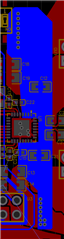
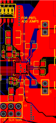
I have successfully integrated the TAS5825M into several designs, but am starting on a new design with some different requirements and thought it would be wise to request a schematic and layout review prior to starting the prototyping. I have attached my Schematics and layout below, but in particular I have a few questions:

1. I have utilized a set of 4 DIP switches to change address between the 4 options. Do you see any issue with that?

2. To be able to switch between PTBL and stereo, I have added headers between the +/- output pours for jumping/unjumping. Are there any reasons why this would cause issues in audio quality or damage the IC?

3. Instead of using a string of vias to connect the PVDD on each side of the amp, I used a pour on the top layer to connect the two sets of PVDD pins. Will this be okay?


Thank you so much for your consideration! I would have posted to the main forums, but for some reason even with my company email the system would not let me post.


Best,

Peter

  • Hi Peter,

    Please refer to the answer as below.

    1. It is no problem to use DIP switch to change address. Note that TAS5825 identify I2C address during power up. So you must choose I2C address by DIP switches before TAS5825 power up.

    2. Whether you use TAS5825 in PBTL mode to achieve mono or use for stereo, there is no problem. Also, it doesn't have impact on audio quality.

    3. It's OK if you connect PVDD on each side of the device by pouring on the same layer. But you can't pour the polygon under the inductances. The signals are coupled to each other.  Besides, I think it's better if you  move  C15 and C22 close to PVDD pin, then put C13, C14, C18 and C19 next to them. The placement principle of capacitator is same for DVDD.

     I don't find some problem in schematic. For PCB layout, you can refer to chapter 10.4 in TAS5825 datasheet to optimize it. Another question is how much the output current of the AMP. I found you use MTP125-1102S1. Dose it have enough current capacity?

    Regards,

    Fengyu

  • Hello Fengyu,

    Thank you very much for the input, I really appreciate it.

    1. Okay, I will take note.

    2. Also good to know, thank you.

    3. Okay, I will try to connect the PVDD pours on the other side of the amp and put the smaller capacitors closer to the PVDD pins. 

    I am planning to provide 20V at 3A available to the amp. The headers are rated to handle 3Amps, so I think I should be okay. How much do you usually expect the amp to draw on the PVDD bus?

    Thank you again so much,

    Peter

  • Hi Peter,

    Do you mean PVDD trace width? It decided  by the  magnitude of the current flowing through PVDD and the PCB current capability.

    Regards,

    Fengyu

  • Hi Fengyu,

    Sorry I accidentally marked the above as the resolution.

    My question is I am wondering if there is a way to calculate how much current will flow through PVDD to the amp. Then after that I would calculate trace width. I want to find the magnitude of the current flow through PVDD.

    Thanks,

    Peter

  • Hi Peter,

    You can roughly estimate the current flow through PVDD by the equation: I ≈ Vpvdd/Rspeaker. And if you want to calculate  more accurately, you can refer to equations from TAS5825 datasheet as below because Ipvdd is equal to current flow through inductor.

    Regards,

    Fengyu

  • Hello Fengyu,

    Thank you very much for the help. I have reworked my layout. I have moved the smaller bypass capacitors closer to the amp instead of the decoupling capacitors like you recommended. Additionally, I now have PVDD routed through 16 vias to the bottom layer instead of under the inductors. Do you see anything wrong with this approach? See the snips below.

    Additionally, is there anything wrong with running a ground pour beneath the inductors or should I have nothing under them?

    Thank you so much,

    Peter

  • Hi Peter,

    There is nothing wrong with your PVDD connection method. TAS5825EVM also let ground pour beneath inductors. So I think it is OK.

    Regards,

    Fengyu