This thread has been locked.

If you have a related question, please click the "Ask a related question" button in the top right corner. The newly created question will be automatically linked to this question.

PCM1864EVM: There is an issue with the audio data collected using TIDA-01454 and C6748EVM

Part Number: PCM1864EVM
Other Parts Discussed in Thread: PCM1864, TIDA-01454

Hello E2E Experts,

Good day.

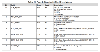
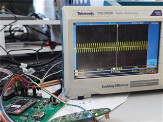
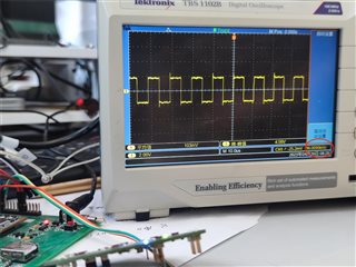
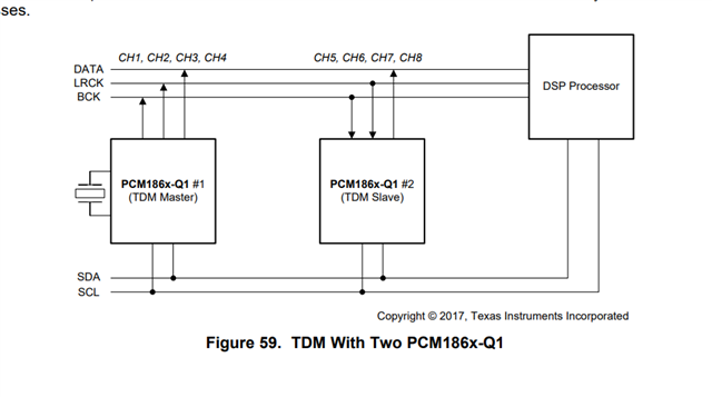
This is the project. The image shows the audio data I found in the memory browser during debugging. Obviously, there is a problem, but I don't know where the problem lies.

AUDIO_MIC_IN.zip

Regards,

CSC

  • I am sorry I am not a specialist on C6748. I can help on any issue regarding PCM1864 DEVICE

  • Hello Sanjay,

    Good day.

    Is the issue more of the C6748 rather than the PCM1864?

    Regards,

    CSC

  • To try answer that question ,I would suggest to take a look at the timings(BCK/LRCK/SCKI) that are going into the PCM1864 chip to see if these are correct

  • Hello Sanjay,

    Good day.

    As shown in the figure, PCM1864 can be configured to automatically configure the clock. But after taking your suggestion, I still went to check my clock configuration. I don't think the problem I'm facing is related to the clock.

    Regards,

    CSC

  • Can you send me your register settings for the clock? i can try to see if they are fine

  • Hello Sanjay,

    Good day.

    Actually, the project I uploaded earlier included the PCM1864 source file, which includes clock settings.I will upload the source file again, which includes the register settings for the clock.

    /****************************************************************************/
    /*                                                                          */
    /*              ���ݴ������ӿƼ����޹�˾                                    */
    /*                                                                          */
    /*              Copyright 2015 Tronlong All rights reserved                 */
    /*                                                                          */
    /****************************************************************************/
    /****************************************************************************/
    /*                                                                          */
    /*              PCM1864��ʼ��                                               */
    /*                                                                          */
    /*              2015��07��20��                                              */
    /*                                                                          */
    /****************************************************************************/
    #include "codecif.h"
    #include "pcm1864_init.h"
    
    /****************************************************************************/
    /*                                                                          */
    /*              �궨��                                                      */
    /*                                                                          */
    /****************************************************************************/
    #define PCM18_RESET                 (0xFE)
    
    #define PCM18_SLOT_WIDTH_32         (0u )
    #define PCM18_SLOT_WIDTH_24         (1u )
    #define PCM18_SLOT_WIDTH_20         (2u )
    #define PCM18_SLOT_WIDTH_16         (3u )
    
    /****************************************************************************/
    /*                                                                          */
    /*              ��������                                                    */
    /*                                                                          */
    /****************************************************************************/
    /**
     *  ����	��λPCM1864
     *
     *  ����	baseAddr :���� PCM1864 �ӿڵĻ���ַ��I2C�Ļ���ַ��
     *
     *  ����	��
     *
     **/
    void PCM18Reset(unsigned int baseAddr)
    {
    	// ѡ�� Page 0
    //    I2CRegWrite(baseAddr, PCM18_P0_REG0, 0);
    
        // ��λ
        I2CRegWrite(baseAddr, PCM18_P0_REG0, PCM18_RESET);
    }
    
    /**
     *  ����	��ʼ�� PCM1864 ����ģʽ�� slot λ��
     *
     *  ����	baseAddr : ���� PCM1864 �ӿڵĻ���ַ��I2C�Ļ���ַ��
     *  		RX_Width: ���� ����Slot ���
     *                              TDM_LRCK_MODE��LRCK Duty Cycle in TDM Mode
     *  		             dataOff  : ����ʱ�ӵ������ص�������Ч���ݵ�ʱ�Ӹ���
     *                              TX_Width: ���� ����Slot ���
     *  		dataType : ������������ģʽ
     *
     *  			dataType ��ֵ��������Ϊ��
     *  	                PCM18_DATATYPE_I2S - I2S ģʽ \n
     *              	PCM18_DATATYPE_DSP - DSP ģʽ \n
     *              	PCM18_DATATYPE_RIGHTJ - �Ҷ���ģʽ \n
     *              	PCM18_DATATYPE_LEFTJ -  �����ģʽ \n
     *
     *  ����	��
     *
     **/
    void PCM18DataConfig(unsigned int baseAddr, unsigned char RX_Width, unsigned char TDM_LRCK_MODE,
                   unsigned char TX_Width, unsigned char dataType)
    {
        unsigned char slot1;
        unsigned char slot2;
        unsigned char temp1;
    
        switch(RX_Width)
        {
            case 16:
                slot1 = PCM18_SLOT_WIDTH_16;
            break;
    
            case 20:
                slot1 = PCM18_SLOT_WIDTH_20;
            break;
    
            case 24:
                slot1 = PCM18_SLOT_WIDTH_24;
            break;
    
            case 32:
                slot1 = PCM18_SLOT_WIDTH_32;
            break;
    
            default:
                slot1 = PCM18_SLOT_WIDTH_24;
            break;
        }
        slot1=slot1<<6;
    
        temp1=TDM_LRCK_MODE<<4;
    
        switch(TX_Width)
        {
            case 16:
                slot2 = PCM18_SLOT_WIDTH_16;
            break;
    
            case 20:
                slot2 = PCM18_SLOT_WIDTH_20;
            break;
    
            case 24:
                slot2 = PCM18_SLOT_WIDTH_24;
            break;
    
            case 32:
                slot2 = PCM18_SLOT_WIDTH_32;
            break;
    
            default:
                slot2 = PCM18_SLOT_WIDTH_24;
            break;
        }
        slot2=slot2<<2;
    
        // ��������ģʽ�� slot λ��
        I2CRegWrite(baseAddr, PCM18_P0_REG11, (slot1 | temp1 | slot2 | dataType));
    
        // ���ô���ͨ������:4
        I2CRegWrite(baseAddr, PCM18_P0_REG12, 0x01);
      
        // TDM��ʽ�£������ź������SCK(BCK)���ӳ�λ��(1bit)
        I2CRegWrite(baseAddr, PCM18_P0_REG13, 0x01);
    
        // TDM��ʽ�£������ź������SCK(BCK)���ӳ�λ��(1bit)
        I2CRegWrite(baseAddr, PCM18_P0_REG14, 0x01);
    }
    
    /**
     *  ����	���� PCM1864 �IJ����ʣ�1��2�ӣ�
     *
     *  ����	baseAddr  : ���� PCM1864 �ӿڵĻ���ַ��I2C�Ļ���ַ��
     *  		RefSource : ѡ�� SCK_or_XTAL, SCK ���� XTAL(XI)
     *  		sampleRate: ������
     *
     *  			sampleRate ��ֵ��������Ϊ��
     *  				FS_8000_HZ ,FS_11025_HZ ,FS_16000_HZ ,FS_22050_HZ ,FS_24000_HZ
     *  				FS_32000_HZ ,S_44100_HZ ,FS_48000_HZ ,FS_96000_HZ ,FS_192000_HZ
     *                                              �˴�LRCK��SCKI��Ƶ�õ���Ϊ192Hz
     *  			                //������ fs �����µ�ʽ�Ƶ���
     *  				//fs = (PLL_IN * [pllJval.pllDval] * pllRval) /(2048 * pllPval).
     *  			���� SCKI  ���ⲿ�������� 	SCKI  = 24576 kHz
     *
     *  ����	��
     *
     **/
    void PCM18SampleRateConfig1(unsigned int baseAddr,  unsigned char RefSource, unsigned char mode,
                               unsigned int sampleRate)
    {
          unsigned char temp;
    
        // PCM18_P0_REG40 Ĭ��ʹ��PLL������SCKΪ�ο�
        
        // ����SCK��Դ(XTAL)����ģʽ����ģʽʱ��Դѡ��(PLL)��
        // ADCԴΪSCK��DSP2ԴΪPLL��DSP1ԴΪPLL (�˴�д��10010110)
        I2CRegWrite(baseAddr, PCM18_P0_REG32, 0x1B);
    
        // ����PLL SCK Output��SCK Out�ı�ֵ���˴�Ϊ2��Ƶ
        I2CRegWrite(baseAddr, PCM18_P0_REG37, 0x01);
      
        // ������ģʽ��SCK��BCK�ı�ֵ���˴�Ϊ1��Ƶ
        I2CRegWrite(baseAddr, PCM18_P0_REG38, 0x00);
    
        // ����BCK��LRCK�ı�ֵ���˴�Ϊ256��Ƶ
        I2CRegWrite(baseAddr, PCM18_P0_REG39, 0xFF);
    
        // ����PLL��Pֵ, P=4
        I2CRegWrite(baseAddr, PCM18_P0_REG41, 0x07);
    
        // ����PLL��Rֵ, R=2
        I2CRegWrite(baseAddr, PCM18_P0_REG42, 0x01);
    
        // ����PLL��Jֵ, J=8
        I2CRegWrite(baseAddr, PCM18_P0_REG43, 0x08);
    
        // ����PLL��Dֵ����8λ�͸�6λ��
        I2CRegWrite(baseAddr, PCM18_P0_REG44, 0);
        I2CRegWrite(baseAddr, PCM18_P0_REG45, 0);
        
        // ����DSP1��ʱ�ӣ�����Ƶ
        I2CRegWrite(baseAddr, PCM18_P0_REG33, 0);
    
        // ����DSP2��ʱ�ӣ�2��Ƶ
        I2CRegWrite(baseAddr, PCM18_P0_REG34, 0);
    
        // ����ADC��ʱ�ӣ�4��Ƶ��
        I2CRegWrite(baseAddr, PCM18_P0_REG35, 0x07);
    
        // ����GPIO0Ϊ����ڣ����SCKO
        I2CRegWrite(baseAddr, PCM18_P0_REG18, 0x04);
        I2CRegWrite(baseAddr, PCM18_P0_REG16, 0x03);
    
        // ����GPIO3Ϊ����ڣ����DOUT2
        I2CRegWrite(baseAddr, PCM18_P0_REG19, 0x40);
        I2CRegWrite(baseAddr, PCM18_P0_REG17, 0x50);
    }
    
    void PCM18SampleRateConfig2(unsigned int baseAddr,  unsigned char RefSource, unsigned char mode,
                               unsigned int sampleRate)
    {
          unsigned char temp;
    
        // PCM18_P0_REG40 Ĭ��ʹ��PLL������SCKΪ�ο�
        
        temp=1<<5;
        // ����SCK��Դ(SCKI)����ģʽʱ��Դ����ģʽ(Slave)
        // ADCԴΪSCK��DSP2ԴΪSCK��DSP1ԴΪSCK������ʱ�Ӽ����
        I2CRegWrite(baseAddr, PCM18_P0_REG32, 0x01);
      
        // ����PLL��Pֵ, P=8
        I2CRegWrite(baseAddr, PCM18_P0_REG41, 0x0F);
    
        // ����PLL��Rֵ, R=2
        I2CRegWrite(baseAddr, PCM18_P0_REG42, 0x01);
    
        // ����PLL��Jֵ, J=8
        I2CRegWrite(baseAddr, PCM18_P0_REG43, 0x10);
    
        // ����PLL��Dֵ����8λ�͸�6λ��
        I2CRegWrite(baseAddr, PCM18_P0_REG44, 0);
        I2CRegWrite(baseAddr, PCM18_P0_REG45, 0);
        
        // ����DSP1��ʱ�ӣ�����Ƶ
        I2CRegWrite(baseAddr, PCM18_P0_REG33, 0);
    
        // ����DSP2��ʱ�ӣ�����Ƶ
        I2CRegWrite(baseAddr, PCM18_P0_REG34, 0x01);
    
        // ����ADC��ʱ�ӣ�8��Ƶ��
        I2CRegWrite(baseAddr, PCM18_P0_REG35, 0x0F);
    
        I2CRegWrite(baseAddr, PCM18_P0_REG18, 0x00);
        I2CRegWrite(baseAddr, PCM18_P0_REG16, 0x00);
    
        // ����GPIO3Ϊ����ڣ����DOUT2
        I2CRegWrite(baseAddr, PCM18_P0_REG19, 0x40);
        I2CRegWrite(baseAddr, PCM18_P0_REG17, 0x50);
    }
    
    /**
     *  ����	��ʼ�� PCM1864 �� ADC �����������
     *
     *  ����	baseAddr  : ���� PCM1864 �ӿڵĻ���ַ��I2C�Ļ���ַ��
     *  		adcGain   : ADC ���������
     *  		
     *
     *  			
     *  			
     *  				
     *  				
     *
     *  ����	��
     *
     **/
    
    void PCM18ADCInit1(unsigned int baseAddr)
    {
    //    unsigned char adc_gain = adcGain/0.5;
    
    // ADCͨ������ѡ��
         //����ΪPage0
        I2CRegWrite(baseAddr, PCM18_P0_REG0, 0x00);  


        // ��ͨ��(CH1L, CH1R, CH2L, CH2R,)ѡ������ģ���źţ��źż����������������
        I2CRegWrite(baseAddr, PCM18_P0_REG6, 0x41);   //L1��������
        I2CRegWrite(baseAddr, PCM18_P0_REG7, 0x41);   //R1��������
        I2CRegWrite(baseAddr, PCM18_P0_REG8, 0x44);
        I2CRegWrite(baseAddr, PCM18_P0_REG9, 0x44);


        // ����ADC��ѡ��ͨ��(Ĭ�ϲ�ѡ��)
        I2CRegWrite(baseAddr, PCM18_P0_REG10, 0x00);
    /**************************************************************************************/
    
    // PGA Value����
        // ����ΪPage0
        I2CRegWrite(baseAddr, PCM18_P0_REG0, 0x00);
    
        // ��PGA(CH1L, CH1R, CH2L, CH2R)��С���ã��ݶ�Ϊ32�ֱ�
        I2CRegWrite(baseAddr, PCM18_P0_REG1, 0x40);
        I2CRegWrite(baseAddr, PCM18_P0_REG2, 0x40);
        I2CRegWrite(baseAddr, PCM18_P0_REG3, 0x40);
        I2CRegWrite(baseAddr, PCM18_P0_REG4, 0x40);
    
        // PGAģʽ���Զ�����ӳ��(Ĭ��)
    
     //   I2CRegWrite(baseAddr, PCM18_P0_REG25, 0x00);
    
    
        // �Զ��������ƣ�
        // ƽ���ı�PGA���������Ƹ�ͨ��PGA��ʹ���������
        // �Զ���������˥����ƽ�������Զ���������ǰ�����������������Զ��������AGC
        I2CRegWrite(baseAddr, PCM18_P0_REG5, 0x86);
    
    
    /*
        // ������PGA(DPGA)��������
        I2CRegWrite(baseAddr, PCM18_P0_REG15, 0x00);
        I2CRegWrite(baseAddr, PCM18_P0_REG22, 0x00);
        I2CRegWrite(baseAddr, PCM18_P0_REG23, 0x00);
        I2CRegWrite(baseAddr, PCM18_P0_REG24, 0x00);
    */
    /**************************************************************************************/
    
    // DSP_CTRL�Ĵ�������(Page.0, 0x71)��
        // ����ΪPage0
    //    I2CRegWrite(baseAddr, PCM18_P0_REG0, 0x00);
    
        // 4ͨ��(Ĭ��)�����ֳ�ȡ�˲���ѡ��ͨ����FIR�����ø�ͨ�˲������ĸ�ͨ��������
        I2CRegWrite(baseAddr, PCM18_P0_REG113, 0x10);
    /**************************************************************************************/
    
    // ���ֻ�����(Digital Mixer)����
        // ����ΪPage1
        I2CRegWrite(baseAddr, PCM18_P0_REG0, 0x01);
    
    // ����Mix1���ĸ�ͨ��������������Ϊ0dB
    
        // ����Mix1_CH1L
        I2CRegWrite(baseAddr, PCM18_P1_REG2, 0x00);  // Mix1_CH1L��ַ
        // ����Mix1_CH1L������
        I2CRegWrite(baseAddr, PCM18_P1_REG4, 0xA0);
        I2CRegWrite(baseAddr, PCM18_P1_REG5, 0x00);
        I2CRegWrite(baseAddr, PCM18_P1_REG6, 0x00);
        //ִ��д������������
        I2CRegWrite(baseAddr, PCM18_P1_REG1, 0x01);
        I2CRegWrite(baseAddr, PCM18_P1_REG1, 0x01);
        I2CRegWrite(baseAddr, PCM18_P1_REG1, 0x01);
    
        // ����Mix1_CH1R
        I2CRegWrite(baseAddr, PCM18_P1_REG2, 0x01);  // Mix1_CH1R��ַ
        // ����Mix1_CH1R������
        I2CRegWrite(baseAddr, PCM18_P1_REG4, 0xA0);
        I2CRegWrite(baseAddr, PCM18_P1_REG5, 0x00);
        I2CRegWrite(baseAddr, PCM18_P1_REG6, 0x00);
        //ִ��д������������
        I2CRegWrite(baseAddr, PCM18_P1_REG1, 0x01);
        I2CRegWrite(baseAddr, PCM18_P1_REG1, 0x01);
        I2CRegWrite(baseAddr, PCM18_P1_REG1, 0x01);
    
        // ����Mix1_CH2L
        I2CRegWrite(baseAddr, PCM18_P1_REG2, 0x02);  // Mix1_CH2L��ַ
        // ����Mix1_CH2L������
        I2CRegWrite(baseAddr, PCM18_P1_REG4, 0xA0);
        I2CRegWrite(baseAddr, PCM18_P1_REG5, 0x00);
        I2CRegWrite(baseAddr, PCM18_P1_REG6, 0x00);
        //ִ��д������������
        I2CRegWrite(baseAddr, PCM18_P1_REG1, 0x01);
        I2CRegWrite(baseAddr, PCM18_P1_REG1, 0x01);
        I2CRegWrite(baseAddr, PCM18_P1_REG1, 0x01);
    
        // ����Mix1_CH2R
        I2CRegWrite(baseAddr, PCM18_P1_REG2, 0x03);  // Mix1_CH2R��ַ
        // ����Mix1_CH2R������
        I2CRegWrite(baseAddr, PCM18_P1_REG4, 0xA0);
        I2CRegWrite(baseAddr, PCM18_P1_REG5, 0x00);
        I2CRegWrite(baseAddr, PCM18_P1_REG6, 0x00);
        //ִ��д������������
        I2CRegWrite(baseAddr, PCM18_P1_REG1, 0x01);
        I2CRegWrite(baseAddr, PCM18_P1_REG1, 0x01);
        I2CRegWrite(baseAddr, PCM18_P1_REG1, 0x01);


        //����ΪPage0
           I2CRegWrite(baseAddr, PCM18_P0_REG0, 0x03);
        //Power down mic bias control
              I2CRegWrite(baseAddr, PCM18_P3_REG15, 0x00);
        //����ΪPage0
                 I2CRegWrite(baseAddr, PCM18_P0_REG0, 0x00);
    
    }
    
    void PCM18ADCInit2(unsigned int baseAddr)
    {
    //    unsigned char adc_gain = adcGain/0.5;
    
    // ADCͨ������ѡ��
         //����ΪPage0
        I2CRegWrite(baseAddr, PCM18_P0_REG0, 0x00);


        // ��ͨ��(CH1L, CH1R, CH2L, CH2R,)ѡ������ģ���źţ��źż����������������
        I2CRegWrite(baseAddr, PCM18_P0_REG6, 0x41);   //L1��������
        I2CRegWrite(baseAddr, PCM18_P0_REG7, 0x41);   //R1��������
        I2CRegWrite(baseAddr, PCM18_P0_REG8, 0x44);
        I2CRegWrite(baseAddr, PCM18_P0_REG9, 0x44);
    
    
        // ����ADC��ѡ��ͨ��(Ĭ�ϲ�ѡ��)
        I2CRegWrite(baseAddr, PCM18_P0_REG10, 0x00);  
    /**************************************************************************************/
    
    // PGA Value����
        // ����ΪPage0
    //    I2CRegWrite(baseAddr, PCM18_P0_REG0, 0x00);  
        
        // ��PGA(CH1L, CH1R, CH2L, CH2R)��С���ã��ݶ�Ϊ32�ֱ�
        I2CRegWrite(baseAddr, PCM18_P0_REG1, 0x40);
        I2CRegWrite(baseAddr, PCM18_P0_REG2, 0x40);
        I2CRegWrite(baseAddr, PCM18_P0_REG3, 0x40);
        I2CRegWrite(baseAddr, PCM18_P0_REG4, 0x40);
     
        // PGAģʽ���Զ�����ӳ��(Ĭ��)
    
     //   I2CRegWrite(baseAddr, PCM18_P0_REG25, 0x00);
    
    
        // �Զ��������ƣ�
        // ƽ���ı�PGA���������Ƹ�ͨ��PGA��ʹ���������
        // �Զ���������˥����ƽ�������Զ���������ǰ�����������������Զ��������AGC 
        I2CRegWrite(baseAddr, PCM18_P0_REG5, 0x86);
    
    
    /*
        // ������PGA(DPGA)��������
        I2CRegWrite(baseAddr, PCM18_P0_REG15, 0x00); 
        I2CRegWrite(baseAddr, PCM18_P0_REG22, 0x00); 
        I2CRegWrite(baseAddr, PCM18_P0_REG23, 0x00);  
        I2CRegWrite(baseAddr, PCM18_P0_REG24, 0x00);  
    */
    /**************************************************************************************/
     
    // DSP_CTRL�Ĵ�������(Page.0, 0x71)��
        // ����ΪPage0
    //    I2CRegWrite(baseAddr, PCM18_P0_REG0, 0x00);  
    
        // 4ͨ��(Ĭ��)�����ֳ�ȡ�˲���ѡ��ͨ����FIR�����ø�ͨ�˲������ĸ�ͨ��������
        I2CRegWrite(baseAddr, PCM18_P0_REG113, 0x10);  
    /**************************************************************************************/
     
    // ���ֻ�����(Digital Mixer)����
        // ����ΪPage1
        I2CRegWrite(baseAddr, PCM18_P0_REG0, 0x01);  
    
    // ����Mix1���ĸ�ͨ��������������Ϊ0dB
    
        // ����Mix1_CH1L
        I2CRegWrite(baseAddr, PCM18_P1_REG2, 0x00);  // Mix1_CH1L��ַ
        // ����Mix1_CH1L������
        I2CRegWrite(baseAddr, PCM18_P1_REG4, 0xA0);
        I2CRegWrite(baseAddr, PCM18_P1_REG5, 0x00); 
        I2CRegWrite(baseAddr, PCM18_P1_REG6, 0x00); 
        //ִ��д������������
        I2CRegWrite(baseAddr, PCM18_P1_REG1, 0x01);  
        I2CRegWrite(baseAddr, PCM18_P1_REG1, 0x01);  
        I2CRegWrite(baseAddr, PCM18_P1_REG1, 0x01);  
    
        // ����Mix1_CH1R
        I2CRegWrite(baseAddr, PCM18_P1_REG2, 0x01);  // Mix1_CH1R��ַ
        // ����Mix1_CH1R������
        I2CRegWrite(baseAddr, PCM18_P1_REG4, 0xA0);
        I2CRegWrite(baseAddr, PCM18_P1_REG5, 0x00); 
        I2CRegWrite(baseAddr, PCM18_P1_REG6, 0x00); 
        //ִ��д������������
        I2CRegWrite(baseAddr, PCM18_P1_REG1, 0x01);  
        I2CRegWrite(baseAddr, PCM18_P1_REG1, 0x01);  
        I2CRegWrite(baseAddr, PCM18_P1_REG1, 0x01);  
     
        // ����Mix1_CH2L
        I2CRegWrite(baseAddr, PCM18_P1_REG2, 0x02);  // Mix1_CH2L��ַ
        // ����Mix1_CH2L������
        I2CRegWrite(baseAddr, PCM18_P1_REG4, 0xA0);
        I2CRegWrite(baseAddr, PCM18_P1_REG5, 0x00); 
        I2CRegWrite(baseAddr, PCM18_P1_REG6, 0x00); 
        //ִ��д������������
        I2CRegWrite(baseAddr, PCM18_P1_REG1, 0x01);  
        I2CRegWrite(baseAddr, PCM18_P1_REG1, 0x01);  
        I2CRegWrite(baseAddr, PCM18_P1_REG1, 0x01);  
    
        // ����Mix1_CH2R
        I2CRegWrite(baseAddr, PCM18_P1_REG2, 0x03);  // Mix1_CH2R��ַ
        // ����Mix1_CH2R������
        I2CRegWrite(baseAddr, PCM18_P1_REG4, 0xA0);
        I2CRegWrite(baseAddr, PCM18_P1_REG5, 0x00); 
        I2CRegWrite(baseAddr, PCM18_P1_REG6, 0x00); 
        //ִ��д������������
        I2CRegWrite(baseAddr, PCM18_P1_REG1, 0x01);  
        I2CRegWrite(baseAddr, PCM18_P1_REG1, 0x01);  
        I2CRegWrite(baseAddr, PCM18_P1_REG1, 0x01);   


        //����ΪPage0
           I2CRegWrite(baseAddr, PCM18_P0_REG0, 0x03);
        //Power down mic bias control
              I2CRegWrite(baseAddr, PCM18_P3_REG15, 0x00);
        //����ΪPage0
                 I2CRegWrite(baseAddr, PCM18_P0_REG0, 0x00);
    
    }
    

    Regards,

    CSC

  • It seems that Register 32 has 1B . It looks that you have set the device in Master Mode.

    In master Mode an external clock is fed to SCK pin(pin 15) and LRCK and BCK appear on pin 16,17.

    Can you please check the frequencies of all three pins? If possible send me scope shots of BCK and LRCK

  • Hello Sanjay,

    Good day.

    I did set the first PCM1864 chip of TIDA-01454 to master mode and the second to slave mode. I checked the SCK and it has the same frequency as the crystal, which is 24.576MHZ.

    I have uploaded two photos of the scope for BCK and LRCK. The first photo is from BCK(24.576MHZ), and the second photo is from LRCK(96KHZ). The problem may not be caused by the clock.

    Regards,

    CSC

  • Is the Scope on AC Coupled mode? I see a portion of the waveform going below zero.

  • Hello Sanjay,

    Good day.

    Actually, the Scope is on DC Coupled mode. The reason the portion of the waveform goes below zero is that I adjusted the vertical position.

    I have another question to ask you. Can TIDA-01454 transmit eight-channel data? How to configure registers if I want to transmit eight-channel data in TDM mode using TIDA-01454?

    Regards,

    CSC

  • It should be possible to set up 2 PCM1864 devices in TDM Mode. The Image above sets up 1 device as a master and the other as a slave.

     I believe both devices can also be used in slave mode if we just feed LRCK and BCK to the chip

    LRCK can be 48Khz and BCK can be LRCK*32*8 =256*LRCK=12.288Mhz. 

    There is an automatic configuration of timing possible if we just feed these LRCK and BCK  timings to the chip

    The Data from 1 chip can be having a TX_TDM_OFFSET(Page 0,0x0D) OF 128

    The other chip can have TX_TDM_OFFSET(Page 0,0x0D) OF 0.

    This will ensure the 2 devices put data in different times.

  • Hello Sanjay,

    Good day.

    Following your approach I have configured the registers as shown in the following figure. However, I am unable to debug. May I get more advice from you about GPIO configuration(Page0,0x10-0x13)?

    Regards,

    CSC

  • Are you using the GPIO pins ? If not you can leave these at default setting