Other Parts Discussed in Thread: TLV320AIC3111
Hello,
I purchased a TLV320AIC3111EVM-K dev kit in order to debug a problem with recovering headset microphone signal on a custom target board that uses the TLV320AIC3111 codec and is running Android. The target board processor is an iMX8MP SoC. The TLV320AIC3111 codec is used for audio out, both speakers and headphones, and for headset microphone input. A WM8904 codec on the SoC is used for support of an internal digital PDM microphone. When a headset with integrated microphone is inserted into the headset jack on the target board, the TLV320AIC3111 and driver detects the headset properly. The problem I am facing is configuration of the codec to recover an audio signal from it.
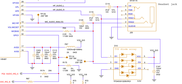
I have attached the relevant sheet of the target board schematic for your reference (target_schematic_p20.pdf).
The audio interface is configured to operate in I2S mode with 12.3 MHz sourced by the processor to the codec. The codec is configured to drive the BCLK and WCLK timing signals at 3.07 MHz and 48 KHz respectively.
The Android system software uses the tlv320aic31xx.c Linux kernel driver to manage the TLV320AIC3111 codec device on the target board. I modified this driver for this application to add support for the headset jack and headset detection, added support for the external headset microphone in capture mode, and a few other miscellaneous features. I also added debug capability, including the ability to set and read individual codec registers, and to dump the entire set of registers.
The attached file reg_recording.txt is a register dump of the codec registers on the target system after the headset has been inserted into the headset jack and the audio record application has been started.
The attached files Android_boot.txt and Android_headset_detect.txt are script files that I assembled by using a logic analyzer to capture the codec I2C traffic issued by the Android system during boot-up (probing and configuring the codec) and during headset insertion and start-up of the audio record application. The ordering of the commands and content of the commands in these script files was created to reproduce how the Android system is managing the codec.
I compared the register contents in the Register Inspector tool after running first the Android_boot.txt script, then inserting the headset into the EVM board headset jack, and then running the Android_headset_detect.txt script. With a few exceptions, the register contents were the same.
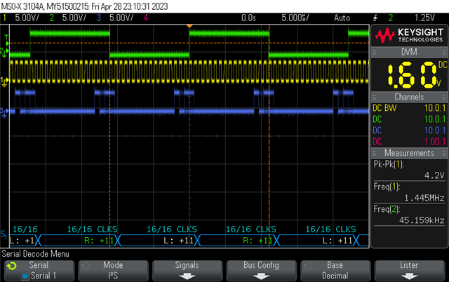
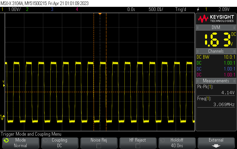
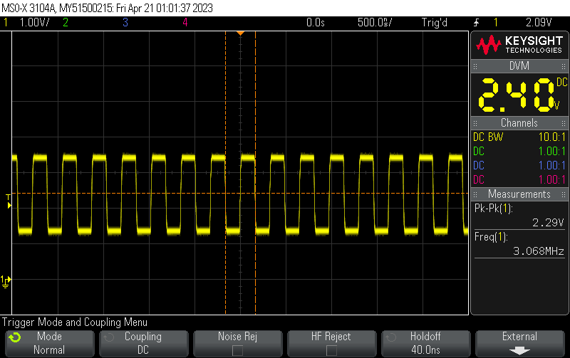
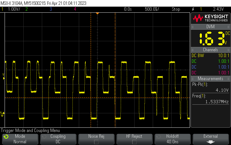
One issue I have run into is that I seem to have contention on the BCLK and WCLK signals on the EVM board after running the scripts. The contention occurs when the commands at lines 74 and 76 in the Android_headset_detect.txt script are executed on the EVM.
I captured this contention on the scope; see waveforms below.
The waveform below (scope_305.bmp) shows the BCLK signal as it appears after just the Android_boot.txt script is executed.
The waveform below (scope_306.bmp) shows how that same signal looks after the Android_headset_detect.txt script is executed, after the first script.
A similar contention also occurs momentarily while the Android_boot.txt script is running. See the waveform below (scope_307.bmp).
I'm guessing that one or more of the jumpers and switches on the EVM is misconfigured to cause this problem.
The jumpers and switches are configured on the EVM board as follows:
Mother board:
SW1-1 -- on
SW1-2 -- on
JMP1 -- shunt installed
JMP6 -- shunt installed to REG (using external 9V power supply for EVM power)
SW3 -- 3.3 V; all other switches set to off
JMP5 -- shunt installed to FSX
J6 -- no shunts on SDA or SCL
JMP3 -- no shunt on SDA
JMP4 -- no shunt on SCL
JMP7 -- shunt from 2 to 3 (also tried 1 to 2, but no difference)
SW2-A1 -- on
SW2-EXT MCK -- on
SW2, all other switches off
Daughter board:
W3 -- no shunt
W2 -- no shunt
scope_307.bmp W21 -- shunt installed
W22 -- shunt installed
W4 -- no shunt
W5 -- shunt installed
W6 -- no shunt
W1 -- shunt between pins 2 and 3
W7 -- shunt between pins 1 and 2
W8 -- shunt between pins 1 and 2
W9 -- shunt between pins 2 and 3
W16 -- no shunt
W17 -- no shunt
W18 -- no shunt
W19 -- no shunt
W20 -- shunt installed
With the jumpers and switches configured as above, the EVM circuitry seems to be configured essentially the same as the circuitry on the target board with the following exceptions:
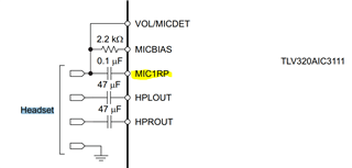
(1) The headset microphone audio input is at MIC1RP on the target board; it is at MICLP on the EVM. I think this does not matter, except that the configuration script was adjusted to make this configuration change.
(2) I notice that there are additional networks consisting of components R19 and C23, and components R20 and C24, on the headphone output signals, that are on the EVM board, but not on our target board. I am not sure what the purpose of these are; they are not shown in the reference circuitry in the TLV320AIC3111 data sheet. Please advise.
At this moment, I am blocked due to the contention problem on the BCLK and WCLK signals described above. After this is resolved, I can try to see if the EVM can receive an audio signal from the headset microphone.
BTW, if there is any additional app notes or other documentation pertaining to the headset circuitry, please attach them.
Also, please let me know if you need any other information from me to clarify the problems I am seeing.
Thanks.
--ken
[  156.402506][ T1750] tlv320aic31xx-codec 5-0018: page 0 reg 3 (0x03) : 0x56
[  156.409811][ T1750] tlv320aic31xx-codec 5-0018: page 0 reg 4 (0x04) : 0x03
[  156.417124][ T1750] tlv320aic31xx-codec 5-0018: page 0 reg 5 (0x05) : 0x91
[  156.424616][ T1750] tlv320aic31xx-codec 5-0018: page 0 reg 6 (0x06) : 0x08
[  156.432290][ T1750] tlv320aic31xx-codec 5-0018: page 0 reg 7 (0x07) : 0x07
[  156.439616][ T1750] tlv320aic31xx-codec 5-0018: page 0 reg 8 (0x08) : 0x80
[  156.446939][ T1750] tlv320aic31xx-codec 5-0018: page 0 reg 11 (0x0b) : 0x88
[  156.454431][ T1750] tlv320aic31xx-codec 5-0018: page 0 reg 12 (0x0c) : 0x82
[  156.461816][ T1750] tlv320aic31xx-codec 5-0018: page 0 reg 13 (0x0d) : 0x00
[  156.469114][ T1750] tlv320aic31xx-codec 5-0018: page 0 reg 14 (0x0e) : 0x80
[  156.476542][ T1750] tlv320aic31xx-codec 5-0018: page 0 reg 15 (0x0f) : 0x80
[  156.484260][ T1750] tlv320aic31xx-codec 5-0018: page 0 reg 16 (0x10) : 0x08
[  156.491718][ T1750] tlv320aic31xx-codec 5-0018: page 0 reg 18 (0x12) : 0x88
[  156.499205][ T1750] tlv320aic31xx-codec 5-0018: page 0 reg 19 (0x13) : 0x82
[  156.506349][ T1750] tlv320aic31xx-codec 5-0018: page 0 reg 20 (0x14) : 0x80
[  156.513455][ T1750] tlv320aic31xx-codec 5-0018: page 0 reg 21 (0x15) : 0x80
[  156.520523][ T1750] tlv320aic31xx-codec 5-0018: page 0 reg 22 (0x16) : 0x04
[  156.527695][ T1750] tlv320aic31xx-codec 5-0018: page 0 reg 25 (0x19) : 0x00
[  156.534749][ T1750] tlv320aic31xx-codec 5-0018: page 0 reg 26 (0x1a) : 0x01
[  156.541831][ T1750] tlv320aic31xx-codec 5-0018: page 0 reg 27 (0x1b) : 0x0c
[  156.548873][ T1750] tlv320aic31xx-codec 5-0018: page 0 reg 28 (0x1c) : 0x00
[  156.556052][ T1750] tlv320aic31xx-codec 5-0018: page 0 reg 29 (0x1d) : 0x0c
[  156.563097][ T1750] tlv320aic31xx-codec 5-0018: page 0 reg 30 (0x1e) : 0x88
[  156.570146][ T1750] tlv320aic31xx-codec 5-0018: page 0 reg 31 (0x1f) : 0x00
[  156.577193][ T1750] tlv320aic31xx-codec 5-0018: page 0 reg 32 (0x20) : 0x00
[  156.585015][ T1750] tlv320aic31xx-codec 5-0018: page 0 reg 33 (0x21) : 0x00
[  156.592479][ T1750] tlv320aic31xx-codec 5-0018: page 0 reg 34 (0x22) : 0x00
[  156.600377][ T1750] tlv320aic31xx-codec 5-0018: page 0 reg 36 (0x24) : 0xc0
[  156.608095][ T1750] tlv320aic31xx-codec 5-0018: page 0 reg 37 (0x25) : 0x00
[  156.615997][ T1750] tlv320aic31xx-codec 5-0018: page 0 reg 38 (0x26) : 0x11
[  156.623638][ T1750] tlv320aic31xx-codec 5-0018: page 0 reg 39 (0x27) : 0x00
[  156.631284][ T1750] tlv320aic31xx-codec 5-0018: page 0 reg 44 (0x2c) : 0x00
[  156.638916][ T1750] tlv320aic31xx-codec 5-0018: page 0 reg 45 (0x2d) : 0x00
[  156.646596][ T1750] tlv320aic31xx-codec 5-0018: page 0 reg 46 (0x2e) : 0x10
[  156.654240][ T1750] tlv320aic31xx-codec 5-0018: page 0 reg 47 (0x2f) : 0x00
[  156.661429][ T1750] tlv320aic31xx-codec 5-0018: page 0 reg 48 (0x30) : 0xcc
[  156.668482][ T1750] tlv320aic31xx-codec 5-0018: page 0 reg 49 (0x31) : 0x00
[  156.676784][ T1750] tlv320aic31xx-codec 5-0018: page 0 reg 51 (0x33) : 0x16
[  156.683980][ T1750] tlv320aic31xx-codec 5-0018: page 0 reg 53 (0x35) : 0x12
[  156.691001][ T1750] tlv320aic31xx-codec 5-0018: page 0 reg 54 (0x36) : 0x03
[  156.698041][ T1750] tlv320aic31xx-codec 5-0018: page 0 reg 60 (0x3c) : 0x01
[  156.705333][ T1750] tlv320aic31xx-codec 5-0018: page 0 reg 61 (0x3d) : 0x04
[  156.712375][ T1750] tlv320aic31xx-codec 5-0018: page 0 reg 63 (0x3f) : 0x14
[  156.719387][ T1750] tlv320aic31xx-codec 5-0018: page 0 reg 64 (0x40) : 0x0c
[  156.726487][ T1750] tlv320aic31xx-codec 5-0018: page 0 reg 65 (0x41) : 0x00
[  156.733619][ T1750] tlv320aic31xx-codec 5-0018: page 0 reg 66 (0x42) : 0x00
[  156.741486][ T1750] tlv320aic31xx-codec 5-0018: page 0 reg 67 (0x43) : 0xe9
[  156.748514][ T1750] tlv320aic31xx-codec 5-0018: page 0 reg 68 (0x44) : 0x6f
[  156.755820][ T1750] tlv320aic31xx-codec 5-0018: page 0 reg 69 (0x45) : 0x38
[  156.763047][ T1750] tlv320aic31xx-codec 5-0018: page 0 reg 70 (0x46) : 0x00
[  156.770144][ T1750] tlv320aic31xx-codec 5-0018: page 0 reg 81 (0x51) : 0x80
[  156.777316][ T1750] tlv320aic31xx-codec 5-0018: page 0 reg 82 (0x52) : 0x40
[  156.784379][ T1750] tlv320aic31xx-codec 5-0018: page 0 reg 83 (0x53) : 0x68
[  156.791494][ T1750] tlv320aic31xx-codec 5-0018: page 0 reg 86 (0x56) : 0xa0
[  156.798636][ T1750] tlv320aic31xx-codec 5-0018: page 0 reg 87 (0x57) : 0x7e
[  156.806027][ T1750] tlv320aic31xx-codec 5-0018: page 0 reg 88 (0x58) : 0x64
[  156.813177][ T1750] tlv320aic31xx-codec 5-0018: page 0 reg 89 (0x59) : 0x08
[  156.820245][ T1750] tlv320aic31xx-codec 5-0018: page 0 reg 90 (0x5a) : 0x32
[  156.827728][ T1750] tlv320aic31xx-codec 5-0018: page 0 reg 91 (0x5b) : 0x00
[  156.834804][ T1750] tlv320aic31xx-codec 5-0018: page 0 reg 92 (0x5c) : 0x06
[  156.842059][ T1750] tlv320aic31xx-codec 5-0018: page 0 reg 93 (0x5d) : 0x00
[  156.849162][ T1750] tlv320aic31xx-codec 5-0018: page 0 reg 116 (0x74) : 0x00
[  156.856253][ T1750] tlv320aic31xx-codec 5-0018: page 0 reg 117 (0x75) : 0x7e
[  156.863366][ T1750] tlv320aic31xx-codec 5-0018: page 1 reg 30 (0x1e) : 0x00
[  156.870385][ T1750] tlv320aic31xx-codec 5-0018: page 1 reg 31 (0x1f) : 0x14
[  156.877554][ T1750] tlv320aic31xx-codec 5-0018: page 1 reg 32 (0x20) : 0x06
[  156.884608][ T1750] tlv320aic31xx-codec 5-0018: page 1 reg 33 (0x21) : 0x00
[  156.891637][ T1750] tlv320aic31xx-codec 5-0018: page 1 reg 34 (0x22) : 0x00
[  156.898793][ T1750] tlv320aic31xx-codec 5-0018: page 1 reg 35 (0x23) : 0x44
[  156.905811][ T1750] tlv320aic31xx-codec 5-0018: page 1 reg 36 (0x24) : 0x9b
[  156.912900][ T1750] tlv320aic31xx-codec 5-0018: page 1 reg 37 (0x25) : 0x9b
[  156.919986][ T1750] tlv320aic31xx-codec 5-0018: page 1 reg 38 (0x26) : 0x7f
[  156.926999][ T1750] tlv320aic31xx-codec 5-0018: page 1 reg 39 (0x27) : 0x7f
[  156.934087][ T1750] tlv320aic31xx-codec 5-0018: page 1 reg 40 (0x28) : 0x04
[  156.941093][ T1750] tlv320aic31xx-codec 5-0018: page 1 reg 41 (0x29) : 0x04
[  156.948169][ T1750] tlv320aic31xx-codec 5-0018: page 1 reg 42 (0x2a) : 0x00
[  156.955187][ T1750] tlv320aic31xx-codec 5-0018: page 1 reg 43 (0x2b) : 0x00
[  156.962247][ T1750] tlv320aic31xx-codec 5-0018: page 1 reg 44 (0x2c) : 0x20
[  156.969260][ T1750] tlv320aic31xx-codec 5-0018: page 1 reg 46 (0x2e) : 0x02
[  156.976335][ T1750] tlv320aic31xx-codec 5-0018: page 1 reg 47 (0x2f) : 0x00
[  156.983410][ T1750] tlv320aic31xx-codec 5-0018: page 1 reg 48 (0x30) : 0x20
[  156.990516][ T1750] tlv320aic31xx-codec 5-0018: page 1 reg 49 (0x31) : 0x80
[  156.997553][ T1750] tlv320aic31xx-codec 5-0018: page 1 reg 50 (0x32) : 0x00
[  157.004958][ T1750] tlv320aic31xx-codec 5-0018: page 3 reg 16 (0x10) : 0x8c
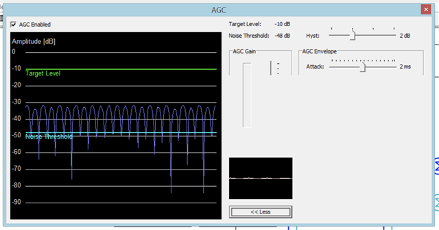
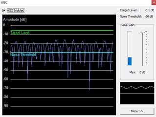
i i2cstd

#     --------------------------------------------------------------- page 0 is selected
w 30 00 00
#      0:1  -- RESET:     s/w reset
> 01
#      0:51 -- GPIO1:     GPIO1 is mapped to INT1 output
w 30 33 16
#      0:48 -- INT1CTRL:  HS detect, BUTTON detect, short circuit, engine interrupts enabled
w 30 30 cc
#      0:27 -- IFACE1:    mode is i2s, wordlength is 16
w 30 1b 0c
#      0:27 -- IFACE2:    BCLK is inverted
w 30 1d 08
#      0:48 -- INT1CTRL:  HS detect, BUTTON detect, short circuit, engine interrupts enabled
w 30 30 cc
#      0:51 -- GPIO1:     GPIO1 is mapped to INT1 output
w 30 33 16
#
#     Note: the following AGC configuration was added manually (not from i2c log)
#      0:83 -- ADCVOL:    ADC coarse gain: 20 dB
w 30 53 28
#      0:86 -- AGCCTL1:   AGC enabled, target level -10 dB
w 30 56 a0
#      0:87 -- AGCCTL2:   2 dB hysteresis, noise threshold -90 dB
w 30 57 7e
#      0:88 -- AGCMAXGAIN: 50 dB maximum gain
w 30 58 64
#      0:89 -- AGCATTACK:  20 ms attack time
w 30 59 78
#      0:90 -- AGCDECAY:  500 ms decay time
w 30 5a b8
#      0:91 -- AGCNSDEB:  0 ms noise debounce time
w 30 5b 00
#      0:92 -- AGCDIDEB:  2 ms signal debounce time
w 30 5c 07
#     --------------------------------------------------------------- page 1 is selected
w 30 00 01
#      1:31 -- HPDRIVER:  OCMV = 1.65 V
w 30 1f 14
#     --------------------------------------------------------------- page 0 is selected
w 30 00 00
#      0:67 -- HSDETECT:  HS detect enabled, 64 ms glitch reject HS only, 8 ms glitch reject button
w 30 43 89
#     --------------------------------------------------------------- page 1 is selected
w 30 00 01
#      1:47 -- MICPGA:    Mic PGA = 0 dB
w 30 2f 80
#      1:36 -- LANALOGHPL: ?
w 30 24 1b
#      1:37 -- RANALOGHPR: ?
w 30 25 1b
#      1:35 -- DACMIXERROUTE: DAC_R is routed to the right-channel mixer amplifier
w 30 23 40
#      1:35 -- DACMIXERROUTE: DAC_L and DAC_R routed to mixer amplifiers
w 30 23 44
#      1:36 -- LANALOGHPL: Set left analog HPL volume to mute
w 30 24 7f
#      1:37 -- RANALOGHPR: Set right analog HPR volume to mute
w 30 25 7f
#      1:38 -- LANALOGSPL: ?
w 30 26 00
#      1:39 -- RANALOGSPR: ?
w 30 27 00
#      1:42 -- SPLGAIN:   SPL driver not muted, gain set to 6 dB
w 30 2a 04
#      1:43 -- SPRGAIN:   SPR driver not muted, gain set to 6 dB
w 30 2b 04
#      1:38 -- LANALOGSPL: Set left SPL gain to 0 dB
w 30 26 80
#      1:39 -- RANALOGSPR: Set right SPR gain to 0 dB
w 30 27 80
#     -----Note: I think boot-up is complete here-----
#              Large (18 second) delay
#              Probably this next part is to set up for audible boot signal:
#     --------------------------------------------------------------- page 0 is selected
w 30 00 00
#      0:4  -- CLKMUX:    PLL_clkin = MCLK, codec_clkin = PLL_CLK
w 30 04 03
#      0:6  -- PLLJ:      J = 8
w 30 06 08
#      0:7  -- PLLDMSB:   D = 1920 (0x780), D(13:8) = 7
w 30 07 07
#      0:8  -- PLLDLSB:   D(7:0) = 80
w 30 08 80
#      0:11 -- NDAC:      NDAC divider is set to 8
w 30 0b 08
#      0:12 -- MDAC:      MDAC divider is set to 2
w 30 0c 02
#      0:13 -- DOSR_LSB:  DAC DOSR MSB set to 0
w 30 0d 00
#      0:14 -- DOSR_MSB:  DAC DOSR LSB set to 0x80
w 30 0e 80
#      0:18 -- NADC:      NADC divider is powered up, set to 8
w 30 12 08
#      0:19 -- MADC:      MADC divider is powered up, set to 2
w 30 13 02
#      0:20 -- AOSR:      ADC AOSR set to 128
w 30 14 80
#      0:30 -- BCLKN:     Set BCLK N divider to 8
w 30 1e 08
#      0:5  -- PLLPR:     PLL Power up, P = 1, R = 1
w 30 05 91
#      0:11 -- NDAC:      Power up NDAC divider (set to 8)
w 30 0b 88
#      0:12 -- MDAC:      Power up MDAC divider (set to 2)
w 30 0c 82
#      0:18 -- NADC:      Power up NADC divider (set to 8)
w 30 12 88
#      0:19 -- MADC:      Power up MADC divider (set to 2)
w 30 13 82
#      0:30 -- BCLKN:     Power up BCLK N divider (set to 8)
w 30 1e 88
#      0:27 -- IFACE2:    BCLK is inverted, BCLK and WCLK active always
w 30 1d 0c
#      0:63 -- DACSETUP:  DAC left and right channels powered, set to corresponding data
w 30 3f d4
#      0:37 -- DACFLAG1:  Wait for left and right DAC channels to power up
f 30 25 1xxx1xxx
#     --------------------------------------------------------------- page 1 is selected
w 30 00 01
#      1:32 -- SPKAMP:    Power up left and right Class D SPL and SPR outputs
w 30 20 c6
#     --------------------------------------------------------------- page 0 is selected
w 30 00 00
#      0:37 -- DACFLAG1:  Wait for left and right Class D outputs to power up
f 30 25 1xx11xx1
#      0:64 -- DACMUTE:   Un-mute DAC outputs
w 30 40 00
#     -----Note: there is a time-out delay here before channels are muted-----
#                         Probably audible boot signal is complete
#      0:64 -- DACMUTE:   Mute DAC outputs
w 30 40 0c
#     --------------------------------------------------------------- page 1 is selected
w 30 00 01
#      1:32 -- SPKAMP:    Power down left and right Class D SPL and SPR outputs
w 30 20 06
#     --------------------------------------------------------------- page 0 is selected
w 30 00 00
#      0:37 -- DACFLAG1:  Wait for left and right Class D outputs to power down
f 30 25 xxx0xxx0
#      0:63 -- DACSETUP:  DAC left and right channels powered down
w 30 3f 14
#      0:37 -- DACFLAG1:  Wait for left and right DAC channels to power down
f 30 25 0xxx0xxx
#      0:27 -- IFACE2:    Disable BCLK and WCLK active when codec powered
w 30 1d 08
#      0:30 -- BCLKN:     Power down BCLK N divider (leave divider set to 8)
w 30 1e 08
#      0:19 -- MADC:      Power down MADC divider (leave divider set to 2)
w 30 13 02
#      0:18 -- NADC:      Power down NADC divider (leave divider set to 8)
w 30 12 08
#      0:12 -- MDAC:      Power down MDAC divider (leave divider set to 2)
w 30 0c 02
#      0:11 -- NDAC:      Power down NDAC divider (leave divider set to 8)
w 30 0b 08
#      0:5  -- PLLPR:     Power down PLL
w 30 05 11
i i2cstd

#     --------------------------------------------------------------- page 0 is selected
w 30 00 00
#      0:44 -- INTRDACFLAG: Wait for headset insert / remove bit to get set
f 30 2c xxx1xxxx
#      0:46 -- INTRDACFLAG2: Wait for headset insert / remove bit to get set
f 30 2e xxx1xxxx
#      0:67 -- HSDETECT:  Wait for headset with microphone detect
f 30 43 111xxxxx
#
#     Headset is detected; pause for next configuration
#
#     --------------------------------------------------------------- page 1 is selected
w 30 00 01
#      1:36 -- LANALOGHPL: ?
w 30 24 1b
#      1:37 -- RANALOGHPR: ?
w 30 25 1b
#      1:40 -- HPLGAIN:   Unmute HPL driver
w 30 28 04
#      1:41 -- HPRGAIN:   Unmute HPR driver
w 30 29 04
#      1:36 -- LANALOGHPL: Set left analog HPL volume to -13.5 dB
w 30 24 9b
#      1:37 -- RANALOGHPR: Set right analog HPR volume to -13.5 dB
w 30 25 9b
#      1:38 -- LANALOGSPL: Set left analog SPL volume to -78.3
w 30 26 ff
#      1:39 -- RANALOGSPR: Set right analog SPL volume to -78.3
w 30 27 ff
#      1:42 -- SPLGAIN:   Mute SPL driver
w 30 2a 00
#      1:43 -- SPRGAIN:   Mute SPR driver
w 30 2b 00
#      1:38 -- LANALOGSPL: Set left analog SPL volume to mute
w 30 26 7f
#      1:39 -- RANALOGSPR: Set right analog SPL volume to mute
w 30 27 7f
#     --------------------------------------------------------------- page 0 is selected
w 30 00 00
#      0:83 -- ADCVOL:    Set ADC coarse volume to -12 dB
w 30 53 68
#      0:82 -- ADCFGA:    Mute ADC
w 30 52 c0
#
#     I believe headphone outputs are on now...
#
#      0:6  -- PLLJ:      J = 8
w 30 06 08
#      0:7  -- PLLDMSB:   D = 1920 (0x780), D(13:8) = 7
w 30 07 07
#      0:8  -- PLLDLSB:   D(7:0) = 80
w 30 08 80
#      0:13 -- DOSR_LSB:  DAC DOSR MSB set to 0
w 30 0d 00
#      0:14 -- DOSR_MSB:  DAC DOSR LSB set to 0x80
w 30 0e 80
#      0:20 -- AOSR:      ADC AOSR set to 128
w 30 14 80
#      0:5  -- PLLPR:     PLL Power up, P = 1, R = 1
w 30 05 91
#      0:11 -- NDAC:      Power up NDAC divider (set to 8)
w 30 0b 88
#      0:12 -- MDAC:      Power up MDAC divider (set to 2)
w 30 0c 82
#      0:18 -- NADC:      Power up NADC divider (set to 8)
w 30 12 88
#      0:19 -- MADC:      Power up MADC divider (set to 2)
w 30 13 82
#      0:30 -- BCLKN:     Power up BCLK N divider (set to 8)
w 30 1e 88
#      0:27 -- IFACE2:    BCLK is inverted, BCLK and WCLK active always
w 30 1d 0c
#      0:63 -- DACSETUP:  DAC left and right channels powered, set to corresponding data
w 30 3f d4
#      0:37 -- DACFLAG1:  Wait for left and right DAC channels to power up
f 30 25 1xxx1xxx
#     --------------------------------------------------------------- page 1 is selected
w 30 00 01
#      1:31 -- HPDRIVER:  Power up HPL and HPR outputs, OCMV = 1.65 V
w 30 1f d4
#     --------------------------------------------------------------- page 0 is selected
w 30 00 00
#      0:37 -- DACFLAG1:  Wait for HPL and HPR outputs to power up
f 30 25 xx1xxx1x
#      0:64 -- DACMUTE:   Un-mute DAC outputs
#
#
w 30 40 00
#      0:6  -- PLLJ:      J = 8
w 30 06 08
#      0:7  -- PLLDMSB:   D = 1920 (0x780), D(13:8) = 7
w 30 07 07
#      0:8  -- PLLDLSB:   D(7:0) = 80
w 30 08 80
#      0:11 -- NDAC:      NDAC divider is set to 8
w 30 0b 08
#      0:12 -- MDAC:      MDAC divider is set to 2
w 30 0c 02
#      0:13 -- DOSR_LSB:  DAC DOSR MSB set to 0
w 30 0d 00
#      0:14 -- DOSR_MSB:  DAC DOSR LSB set to 0x80
w 30 0e 80
#      0:20 -- AOSR:      ADC AOSR set to 128
w 30 14 80
#     --------------------------------------------------------------- page 1 is selected
w 30 00 01
#      1:47 -- MICPGA:    Mic PGA = 0 dB
w 30 2f 00
#      1:46 -- MICBIAS:   Mic Bias = 2.5 V
w 30 2e 02
#
#     Note: target board uses MIC1RP instead of MIC1LP here
#      1:48 -- MICPGAPI:  MIC1LP P-term = 10k
w 30 30 40
#      1:49 -- MICPGAMI:  CM M-term = 10k
w 30 31 40
#     --------------------------------------------------------------- page 0 is selected
w 30 00 00
#      0:81 -- ADCSETUP:  Power up ADC
w 30 51 80
#
#     Note: on target board ADC overflow flag is set here
#
#      0:36 -- ADCFLAG:   Wait for ADC power up and gain applied flags
f 30 25 11xxxxxx
#      0:82 -- ADCFGA:    Unmute ADC, fine gain = -0.4 dB
w 30 51 80