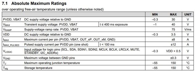
This thread has been locked.

If you have a related question, please click the "Ask a related question" button in the top right corner. The newly created question will be automatically linked to this question.

TAS6422-Q1: (Important) Inquiries about Overtemperature Shut-down and Overcurrent Shut-down

Part Number: TAS6422-Q1

Hi, TI support team

The customer encountered the following problems while using the product.

[problem]

- Product dead (burned, product destroyed), PVDD and GND short, Audio output ch and GND short

[condition]

- output power : 130~140W

-Load : 2ohm

[inquiry]

Due to a problem with some products, we plan to request a defect analysis.

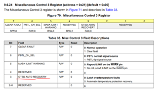
1. Overcurrent shut-down

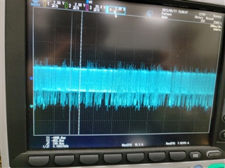
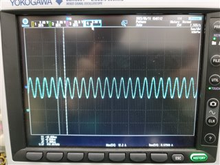
The waveforms below are in normal operation, and the WARN pin, FAULT pin, and Audio output were measured while increasing the output power (current).

(Normal operation, 4A, WARN high, FAULT high)

(Normal operation, 7A, WARN low, FAULT high)

(Normal operation, 7A, WARN low, FAULT high)

As the current increases, the WARN pin operates from high to low, but the FAULT pin does not operate despite increasing the power to 15A.

Why doesn't the FAULT pin work?

Is it normal that it doesn't work?

The cause of the above problem (IC burned) is expected to be caused by overcurrent, but are there other causes?

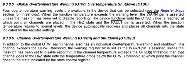
2. Overtemperature shut-down

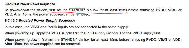
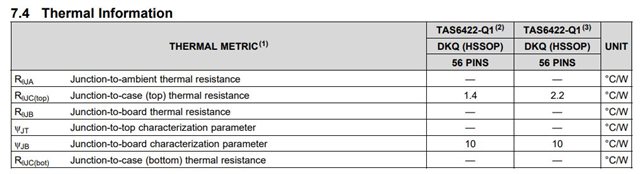
Thermal information is not described in detail in the datasheet.

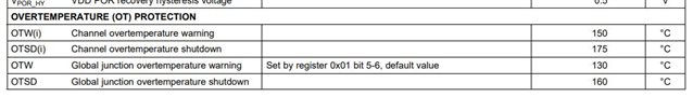
The shut-down operation of the product is assumed by thermal protection.

A heatsink is applied, and the temperature of the heatsink is operating at 130 degrees.

In the condition below, please inform the operating junction temperature.

- Low temperature (-40 degree)

- Room temperature (25 degree)

- High temperature (60 degree)

Thanks.

Regards,

MJ

  • Hi, TI support team

    I have an additional question.

    This is a query about "a minimum of 20cycles" in the "clip detect" part specified in the datasheet.

    Approximately how long is each cycle?

    Thanks.

    Regards,

    MJ

  • Hi MJ

       The OC protection is at the output side, not at the PVDD input side. I find from your waveform, you already works in clipping but still not trigger OC, it means your PVDD and load combination won't trigger OC level, no point to use such clipped output to do this test. If you want to check the OC protection function, just short the output to GND and start PLAY large power would be fine.

       About the thermal value, the junction to top is the most important value, could use it to do the design. The heatsink 130C seems extremely large, from experience, the die temperature should already close to OT shutdown point. Most of design would give some margin to the protection point, usually 30C margin would be the normal using.

    Approximately how long is each cycle?

      The cycle means the audio signal cycle, it depends on the frequency of the audio you are using now.

  • Hi, Shadow

    This is an OCSD-related inquiry.

    There is a setting part related to load overcurrent protection in the datasheet.

    The setting of the OC control register defaults to level 2.

    When the load output is 130W, the output current is confirmed to be approximately 8A.

    The OC control was changed to level 1 and tested.

    I tested with the same output, but the FAULT pin still doesn't work.

    Do I need a setting to operate the FAULT pin?

    Why doesn't the FAULT pin work?

    Thanks.

    Regards,

    MJ

  • Hi, shadow

    Application is designed with PBTL.

    If you give me your email address, I will share the circuit diagram.

    Thanks.

    Regards,

    MJ

  • Hi, Shadow

    This is a series of questions.

    If the FAULT pin operates, does the register below report normally?

    7th bit: 0 -> 1

    6th bit: 0 -> 1

    Thanks.

    Regards,

    MJ

  • Hi MJ

      If you using PBTL, the output current need to reach double of the OC level to trigger the fault, it's hard to trigger this fault by normal using. As I said, you may need to short output to GND to check this function. If the OC fault really happens, the FAULT pin will behave as expected.

    If the FAULT pin operates, does the register below report normally?

       Yes, the register will also report the current fault conditions. And we would recommend to check the register value to find out what fault is triggered. 

       My e-mail is shadow-he@ti.com, it's OK we transfer to e-mail about this problem and close here.

  • Hi, Shadow

    Thank you for your answer.

    Does the WARN reporting condition also double?

    As I said, I am inquiring because WARN is being reported in OCL levle1 and level2.

    If the WARN level of OCL also doubles in PBTL, it is possible that what is currently being reported is due to another factor (overtemp.).

    Is that right?

    Thanks.

    Regards,

    MJ

  • Hi, Shadow

    I requested a circuit diagram review with the link below.

    https://e2e.ti.com/support/audio-group/audio/f/audio-forum/1224822/tas6422-q1-schematic-review-request

    We are reviewing the product as shown in the circuit diagram attached to the inquiry.

    Is there something wrong with the circuit diagram?

    Please confirm.

    Thanks.

    Regards,

    MJ

  • Hi MJ

    Does the WARN reporting condition also double?

    Yes, it's also doubled.

    If the WARN level of OCL also doubles in PBTL, it is possible that what is currently being reported is due to another factor (overtemp.).

    From your description, this is most possible. You could read the register 0x13 to make sure. The WARN will also report to registers.

    Is there something wrong with the circuit diagram?

    I'll check and reply on that Thread.

  • Dear, Shadow

    Thanks.

    Is it possible to share the high/low side FET specifications on the audio output side? (It is confirmed that it is not listed in the datasheet.)

    The spec I want to know is the Current spec.

    Please check that.

    Thanks.

    Regards,

    MJ

  • Dear, Shadow

    This is an additional inquiry.

    I am curious about the order in which the product operates in an environment where OCSD or OTSD occurs.

    - Is it correct that the product is shut-down under the conditions where OCSD and OTSD occur?

    - Does the action (report) of the FAULT pin occur before shut-down?

    - Are the FAULT register and FAULT pin operating before shut-down?

    Thanks.

    Regards,

    MJ

  • Hi, Shadow

    After the TAS6422 detects the OTSD status and enters the Hi-Z status, does the audio output operate automatically?

    Or, should it be operated again through an external reset?

    Looking at the datasheet below, there are some parts that are not clear.

    Thanks.

    Regards,

    MJ

  • Dear, Shadow

    I2S Audio source is being input.

    Are there any restrictions on the input level of the audio source?

    Thanks.

    Regards,

    MJ

  • Dear, Shadow

    Among the defective products, the TAS6422-Q1 was found to have burnt traces in the PVDD power section.

    In this regard, please confirm the following information.

    Among the contents of the absolute maximum ratings of the datasheet, the contents of the PVDD current are as follows.

    - Imax = +-8A

    - Imax_pulsed = +-12A

    As mentioned earlier, the TAS6422-Q1 is designed and used as a PBTL, and at the rated output, an output of approximately 130W is measured, and the

    PVDD_current at this time is as shown in the figure below.

    - Ipeak = 15.3A

    - Ipeak_pulsed = 12.2A (2.4us)

    PVDD, OCL, and OCSD seem to be related.

    OCL and OCSD are said to double the detection level when designed with PBTL.

    Does the use of current supplied by PVDD not change from the value specified in the datasheet?

    As reported above, the current PVDD side current is being input very high.

    What are some bad symptoms that can occur in this situation?

    Thanks.

    Regards,

    MJ

  • Hi MJ

    The spec I want to know is the Current spec.

    I'm sorry that we don't have document about it. The value we could provided is the OC point, maximum 9A, could be guarantee this current won't damage the FET.

    - Is it correct that the product is shut-down under the conditions where OCSD and OTSD occur?

    Yes, product will shutdown directly.

    - Does the action (report) of the FAULT pin occur before shut-down?

    - Are the FAULT register and FAULT pin operating before shut-down?

    Shutdown will be more quickly to prevent damage happens. Report to FAULT pin will through additional circuit, may delay several ns. Report to register will need to go through additional digital circuit, will have additional delay, also several ns.

    After the TAS6422 detects the OTSD status and enters the Hi-Z status, does the audio output operate automatically?

    Or, should it be operated again through an external reset?

    By default settings, OTSD will not auto recover, you'll need to use external reset. Could set the function in register 0x21.

    Are there any restrictions on the input level of the audio source?

    I2S is the digital input, 0dBFS is the maximum level when normal using. Higher than this value, you'll get clipping output, but won't cause damage. So no strict restriction on this.

    PVDD_current at this time is as shown in the figure below.

    - Ipeak = 15.3A

    - Ipeak_pulsed = 12.2A (2.4us)

    This value seems has some problem. As you said you are using 2ohm load and want to get 130W to 140W output. Then the PVDD voltage should be around 24V, right? Otherwise the output will clip too much. The current from you picture seems has 12.2A peak and 8.67A rms, It's already around 200W at PVDD supply. Our device won't have so large power loss. Could you please double check?


    I think you are trying to find out the reason for burn out right? From our experience, this issue mostly caused by bad PCB layout and too much ripple voltage happens at the PVDD and OUTPUT side, cause the voltage stress higher than device's ability. Could you please try to capture the voltage at both PVDD pin and OUTPUT pin of our device, when max power using. And could you also share the PCB layout of the customer's board?

  • Dear, Shadow

    I have sent you the materials needed for review by e-mail.

    For the AMP part design, SCH, PCB layout, and BOM were sent by e-mail.

    This is a customer inquiry.

    Q. Are there many products with the same spec as the TAS6422-Q1 for pin pitch of TI's Power AMP products?

    Doesn't the TAS6422-Q1 product have a particularly narrow pitch?

    Thanks.

    Regards,

    MJ

  • Dear, Shadow

    Please check the inquiries below.

    1. Power up/down sequence inquiry

    - The information in the datasheet is as follows.

    Power up: VBAT -> VDD -> PVDD

    Power down: PVDD -> VDD -> VBAT

    If PVDD is supplied before VDD during power up, or if PVDD is removed later than VDD during power down, what effect does it have on the product?

    Is there a possibility that the product will burn?

    Is there a possibility that the product will be burned or defective when PVDD is still being supplied with VDD removed?

    2. Volume control register inquiry

    Currently, customers are using TAS6422-Q1 as PBTL.

    Can I set the volume control register only for CH1?

    Or, should CH1 and CH2 be set identically?

    What problems can occur if only CH1 is set?

    Please confirm.

    Thanks.

    Regards,

    MJ

  • Hi MJ

    Doesn't the TAS6422-Q1 product have a particularly narrow pitch?

    It used DKQ56 package, TAS642x all used this one, and in the future we may also use this one in other devices.

    If PVDD is supplied before VDD during power up, or if PVDD is removed later than VDD during power down, what effect does it have on the product?

    Is there a possibility that the product will burn?

    Is there a possibility that the product will be burned or defective when PVDD is still being supplied with VDD removed?

    For incorrect sequence, indeed can't provide 100% guarantee by us. Although from the validation test from our side, incorrect sequence won't directly cause damage. But our design team thinks the risk will increase, when mass production, may results in failure rate increase. 

    Currently, customers are using TAS6422-Q1 as PBTL.

    Can I set the volume control register only for CH1?

    In PBTL, only set Volume for CH1 would be fine. CH2 volume won't take effect.

  • Hi, Shadow

    Please check the additional inquiries below.

    The materials reviewed by the customer are attached.

    ACC OFF_ON waveform.xlsx

    Please check item 1 of the attached file (D-AMP PWM status when ACC is off).

    It seems to work ideally after Stand-by is turned off.

    1. A waveform that seems to oscillate is confirmed.

    2. PWM restarts and turns off.

    3. The amplitude of the restarted PWM is different.

    The above three conditions are occurring randomly.

    Q1. What could be the cause of the above symptoms?

    Q2. Please let me know if there is a way to prevent these symptoms from happening.

    Q3. Can these symptoms affect the power stage (PVDD) to fail?

    Q4. Is lasting damage applied?

    Please ASAP.

    Thanks.

    Regards,

    MJ

  • Hi MJ

      Please raise a new thread next time when you have new problem. 

    Q1. What could be the cause of the above symptoms?

    Only when FAULT happens, the PWM stops.

    Q2. Please let me know if there is a way to prevent these symptoms from happening.

    Please read the device's register value, check what FAULT happens, and find out the reason.

    Q3. Can these symptoms affect the power stage (PVDD) to fail?

    Won't damage device, normal protection.

    Q4. Is lasting damage applied?

    No.

  • Hi, Shadow

    It's been a while, but sorry for asking again.

    I would like to ask you a further question.

    The above problem has not been resolved yet, and we would like to ask you additional questions about the power sequence among the previous inquiries.

    In order to solve the problem that VBAT, PVDD, and VDD are applied at almost the same timing, which was a problem in the past, the sequence was

    designed by adding FET to the PVDD input line.

    Please see the timing chart below.


    Some of the previous inquiries have been answered as follows.

    It was applied as a countermeasure to eliminate the possibility of defects in mass production.

    Q1. Will there be any problems when applied to the sequence?

    Q2. There is no timing chart for Power ON/OFF sequence in the datasheet of TAS6422-Q1. Is there a separate timing chart?

    If so, please share. If there is no separate timing chart, will there be any problem if only the sequence is kept? (Related to the question in Q1)

    Thanks.

    Regards,

    MJ

  • Hi MJ

       The power on sequence seems no problem. About the power off, they didn't make very clear at which PVDD threshold will turn off DVDD, do they have very specific control sequence about this point? 

       Although datasheet didn't give waveform of turn on/off sequence, but it has descriptions. The importance about power off sequence, is to pull down STANDBY pin at least 15ms before any power supply goes down. Please make sure we follow this instructions.

       And could you please raise a new Thread next time, or you could also e-mail to us directly. shadow-he@ti.com