This thread has been locked.

If you have a related question, please click the "Ask a related question" button in the top right corner. The newly created question will be automatically linked to this question.

SRC4382: I2C write issue

Part Number: SRC4382
Other Parts Discussed in Thread: SRC4392

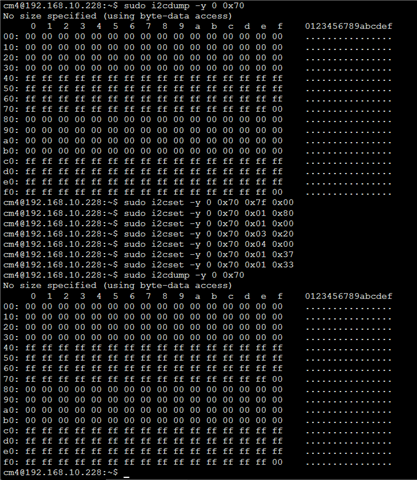
I've a strange issue on writing SRC4382 registers via I2C.

To configure the registers I'm using the i2c-tools application.
The first write is to the Page selection register 0x7f 0x00 (to configure control and status registers)

Reading back this register the value corresponds to the configured value (also if the page selection value  is configured with a value different from 0x00)

After that I write the register 0x01 with 0x3F value to exit from power down status.

Reading back this register the value remains to 0x00.

This issue happens for all registers except the 0x7F and the 0x00 (that in datasheet is declared as reserved register).

Do you have an idea about the cause and what I can check?
I've looked at the I2C bus and seems that aren't any analog or protocol issue on I2C signals.

NB: the I2C bus runs at 40KHz.

Thanks

  • Hello , thanks for reaching out. Your I2C bus is ok and well within the range. Regarding power-down and Reset, Datasheet reads:

    Upon reset initialization, all functional blocks of the SRC4382 default to the powered-down state, with the exception of the SPI or I 2 C host interface and the corresponding control registers. The user may then program the SRC4382 to the desired configuration, and then release the desired function blocks from the power-down state utilizing the corresponding bits in control register 0x01.

    So based on the above,  the following sequence should be used to initialize SRC4382.

    1. Apply power and external reset.

    2. Write all control registers on Page 0 except register 0x01.

    3. Apply MCLK, as well as any audio clocks desired for Ports A and B.

    4. Write register 0x01 on Page 0 to power up the desired blocks.

    A sample code can be 

    # MASTER RESET FOR SRC (48kHz)

    # Page 0 = DEFAULT for Control

    # Write to page 0

    w E0 7F 00

    d 100

    w E0 01 80       # Register 01, Bit 7 = 1 resets to default

    d 100               # Delay 0.1 sec to allow part to reset

    w E0 01 00      # Register 01, Bit 7 = 0 for normal operation

    d 100

    *****Add  all instructions for all registers and then enable the desired function block using reg 01 , for example 

    .....

    w E0 03 20   #  I²S Port A: Clock Slave, 24 Bit Audio MSB, Output Signal from Receiver - NOT from SRC
    w E0 04 00   # I²S Port A: MCLK Source = MCLK; MCLK Freq = 128x LRCLK (MCLK Freq other than 128x just for Master Mode operation)
    ....

    ...

    ...

    ****  then enable the blocks you want. For example 

    w E0  01 37  // switch on SRC, Receiver, Transmitter, I²S Port A

    Regards,

    Arash

  • Hello, thank for the reply. I'm a bit confused about the registers readback possibility..
    For what reason, reading back the registers (after a write) the content seems to be at default value?
    See the screenshot below: after the external reset I read all the registers value (they are at default values)
    After that I write the registers suggested by you, but on the next registers dump the values hasn't changed. I don't expect that this is a normal behaviour, right? Moreover seems that, after programming the registers, the SRC4382 not detect the AES input (lock and ready LEDs are off)
    NB: I need to use the SRC4382 in master mode and receive only, so I don't apply any external signals on the I2S port "A" (I expect to have the I2S signals output from the SRC4382).

  • Hello,

    if you can change the page number and can read it back, then your I2C is working,  To confirm that you are writing into registers,  can you monitor the I2C signals and verify the acknowledge is happening.

    I think most probably you are still resetting the registers into their default configuration. Please make sure you are not resetting the registers by accident. Also switch to another page and try to write and read on the other pages and see what happens.

    Here is a full sample script to initialize the device which should work fine ( I assume your IC address is correct)

    1. Apply power and external reset.

    2. Write all control registers on Page 0 except register 0x01.

    3. Apply MCLK, as well as any audio clocks desired for Ports A and B.

    4. Write register 0x01 on Page 0 to power up the desired blocks.

    5. Disable DIT buffer transfers by setting the TXBTD bit in register 0x08, Page 0, to a 1.

    6. Write 0x02 to register 0x7F to set Page 2 as the active page.

    7. Write data to the DIT C and U buffers on Page 2 as desired.

    8. Write 0x00 to address 0x7F to set Page 0 as the active page.

    9. Enable DIT buffer transfers by setting the TXBTD bit in register 0x08, Page 0, to a 0.
    This will update the DIT TA buffer with the data written to Page 2 registers.

    Example for Implementation of above:

    1. External reset

    2. Setting control registers on page 0 (it's always register address first, then data [all values in hex])

    w e0 7f 00 //Set Register Page 0
    w e0 03 20 // I²S Port A: Clock Slave, 24 Bit Audio MSB, Output Signal from Receiver - NOT from SRC
    w e0 04 00 // I²S Port A: MCLK Source = MCLK; MCLK Freq = 128x LRCLK (MCLK Freq other than 128x just for Master Mode operation)
    w e0 07 00 // Clock Start Output; Transmitter MCLK Divider == FPGA CLK / 128
    w e0 09 01 // Transmitter Channel State Update via SPI
    w e0 0d 00 // Receiver Input == RX1, Ref CLK RXCKI (ext.)
    w e0 0E 00 // Receiver Mute if No CLK, Superclock on ext. Pin, CLK Divider = 4
    // Receiver PLL Ref Clk according Data Sheet (Table 4, S.60)
    w e0 0F 22
    w e0 10 00
    w e0 11 00
    //
    w e0 2D 02 // SRC Source == Receiver, ref. CLK FPGA

    3. Enable clock (mclk, frame sync, sample clock)

    4. w e0 01 37 // switch on SRC, Receiver, Transmitter, I²S Port A


    Here is the script for steps 5 to 9:


    w e0 08 08 // disable the DIT buffer transfer

    w e0 7f 02 // set page to 2

    w e0 2e ee // write ee to reg 2e on page 2

    w e0 2f ff //write ff to reg 2f on page 2

    w e0 7f 00 //change the page back to 0

    w e0 08 00 // enable the DIT buffer transfer

    w e0 7f 02 // switch back to page 2

    r e0 2e 01 // read back reg 2e on page 2

    r e0 2f 01 // read back reg 2f on page 2

    w e0 7f 00 // set page to page 0

    Regards,

    Arash

  • Hi Arash,

    thank you for your explanation, but I still have the problem... The I2C transaction is correct (ACK arrives). 
    Reading back any register (except 0x7F) returns 0x00, even if previously was written with a different value.
    The register 0x7F works as expected (changes the value and reading back return the correct value). Monitoring all the I2C transactions shown no problems on read/write commands. Seems that internally the registers will be not updated. Maybe some mistake in the hardware connections? Some wrong connection or clock loss?

  • Hello Giuseppe, 

    I tested a random script ( attached below)  with the EVM and I was able to  write and read multiple registers correctly. I attached the script  just in case you want to give it a shot with the script.  For this test I only powered up the device and send the I2C command via I2C and PPC3 tool.

    And the script is SRC4392_STATUS_I2C.txt: 

    # sample I2C script
    # set interface mode to i2c fast
    i i2cfast
    # set register page to 0
    w e0 7f 00
    # dir setup is default with automute for loss of lock condition
    w e0 0d 00
    w e0 0e 09
    # pll1 p is 2 j is 8 d is 0
    w e0 0f 22
    w e0 10 00
    w e0 11 00
    # unmask dir status registers
    w e0 16 fe
    w e0 17 01
    # setup dir interrupt mode
    w e0 18 00
    w e0 19 00
    w e0 1a 00
    # dit setup with 512fs rxcko for 48kHz frame rate
    # dir provides v and c and u data
    w e0 07 f4
    w e0 08 00
    w e0 09 06
    # power up the dir and dit
    w e0 01 26
    b
    # read DIR status registers
    r e0 92 04
    b
    # read DIR status registers
    r e0 92 04
    b
    # read DIR status registers
    r e0 92 04
    b
    # read DIR status registers
    r e0 92 04
    b
    # read DIR status registers
    r e0 92 04
    b
    # read DIR status registers
    r e0 92 04
    b
    # read DIR status registers
    r e0 92 04
    b
    # read DIR status registers
    r e0 92 04
    b
    # read DIR status registers
    r e0 92 04
    b
    # read DIR status registers
    r e0 92 04
    b
    # dummy write
    w e0 7f 00
    

    Since you confirmed the I2C sends the acknowledgment, and you can change register 0x7f,  I seems to me I2C is working fine.

    Have you tried to program the part using PPC3 ( I used it and you can get it from TI.com for free), 

     And finally have you replaced  the device just to verify it is not the device issue?  


     Regards,

    Arash