This thread has been locked.

If you have a related question, please click the "Ask a related question" button in the top right corner. The newly created question will be automatically linked to this question.

OPA1679: Share common input and use two amp with different gain

Part Number: OPA1679
Other Parts Discussed in Thread: TINA-TI, TLV320ADC5140, , TLV9154

HI team,

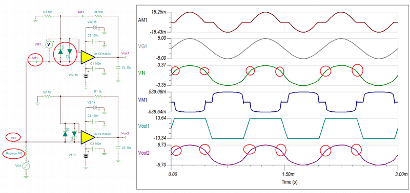
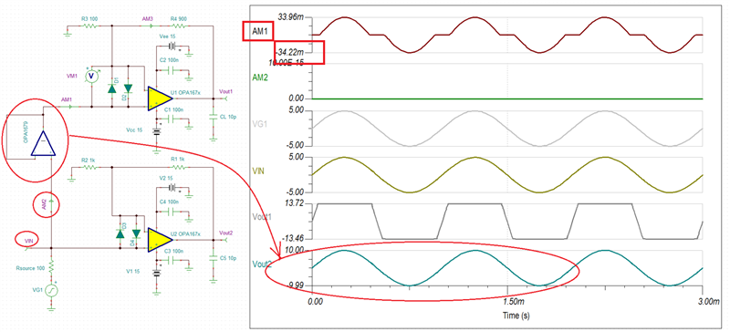
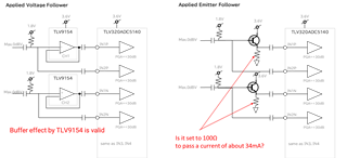
Customer wants to use dual opamp which share common input. Because of difference gain in these opamps, one opamp distortion affects the another opamp through feedback loop.

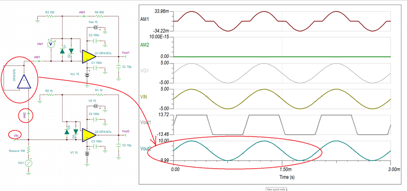
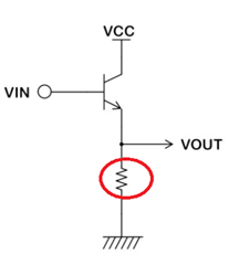
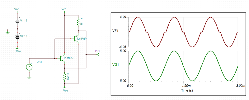
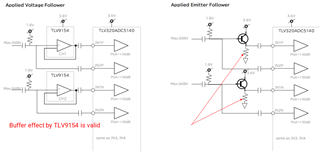
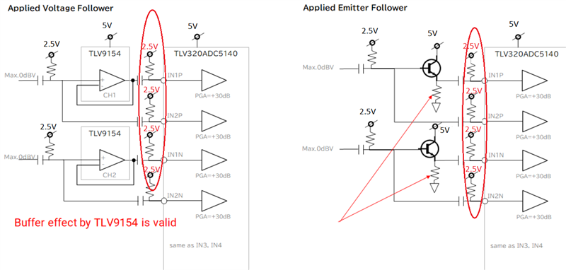
Is there good solution to avoid it? like voltage follower or emitter follower

ex:)

Ch1 Vin -> opamp (inverting amp) -> Vout (G = XX)

Ch2 Vin -> opamp (inverting amp) -> Vout (Gain = YY)

When Ch1 opamp is clipped, the distrotion affects Ch2. They want to make them independent.

Hayashi

  • Hi Hayashi,

    It would be useful for you to show the schematic of two configurations showing the actual gains. In any case, the issue is related to the back-to-back input protection diodes that get turn on when you push Vout1 against its rail - see below.

     H

    Because of the finite source impedance, Rsource, when D1 or D2 gets forward biased (see AM1) while Vout1 gets too close to its rail, it causes a drop across Rsource distorting the input signal, Vin - see below.

    A one simple solution would be to buffer the op amp that gets pushed into non-linear operation - see below.  Even though D1 or D2 draw current, it is supply by the buffer and AM2 stays close to zero, thus eliminating the distortion of Vin.

    Below I have attached Tina-TI schematic for your convenience.

    Hideki OPA1679.TSC

  • Dear Marek-san

    Mr. Hayashi's question is my request. 
    So, I would like to ask a question on behalf of Mr. Hayashi.

    Thank you for your reply.
    I was able to understand this phenomenon by your explanation of the internal circuit and the execution of the simulation.

    If it is the effect of the protection diode, is it difficult to avoid it with a resistor or the like?
    Experiments have confirmed that the voltage follower is effective in avoiding this problem.
    However, op amps are costly due to the number of inputs to care for.
    Therefore, if possible, we would like to replace it with an emitter follower.
    Also, in order to maximize the SNR of the TLV320ADC5140, we are considering using an input impedance of 2.5kΩ (register setting).
    What is the desired level of the emitter resistance of the emitter follower circuit in this case? Please answer.


  • In order to avoid the distortion caused by the railing of one of the op amp, the buffer must be able NOT only source but ALSO sink high current level (see AM1 showing dual polarity signal level), which is not possible with emitter follower circuitry shown above where sinking magnitude is limited to (Vin-Vbe)/R.  One way around the issue would be to use an op amp with no back-to-back input protection diodes like TLV4197 (see below) with THD better than OPA1679 but higher 1ku price.

  • Dear Marek-san

    Thank you for your reply.
    Where in the datasheet is the "see AM1 showing dual polarity signal level" you say?
    Also, it says that it sinks a large current, but what is the current value?
    When you say that it is impossible with an emitter follower, do you mean that it is impossible even if the emitter resistance is reduced?
    (Even if it is realized by reducing the emitter resistance, it may be realistic because the current consumption will increase.)

    I used your company's TLV9154 in my experiments with voltage followers.
    The effect was as expected, but does this operational amplifier have a protection diode?

  • Hi Kasugai-san,

    The AM1 dual polarity current is shown in your specific application - see in red rectangular box below (-34.22 mA).  However, since you did not share the details of your application nor any information about required output drive, there is no way for me to choose the value of the emitter resistor.

    For the negative input signal, VG1, the NPN emitter follower shown above will be turned off and thus would not allow you to pass the input signal.  Thus, you would have to add in parallel PNP emitter follower, which would have a dead zone (large distortion) when the VG1 is just few hundred millivolts - see below. Therefore, you would have to implement a discrete class AB output stage that would be more expansive than using a monolithic op amp.

    Unlike OPA1679, TLV9154 does NOT have back-to-back input protection diodes (see below) so you could use it in your application.

  • Thank you for your opinion.

    At least the buffering by TLV9154 was found to be effective.

    I am attaching my design information.
    The dead zone you're talking about is the distortion caused by the NPN and PNP turning on at the same time when the input is very close to zero in dual power supply applications, right?

    The circuit is operated with a single power supply, and I intend to apply a bias voltage to the input of the emitter follower.
    As a result, the NPN transistor is ON even during negative input, so I think there is no dead zone.
    Also, I understand that an emitter resistance of about 100Ω is required to flow a sink current of 34mA or more. is my understanding correct?


  • TLV9154 does not have back-to-back input protection diodes and thus your circuit should work fine without the buffers.

    In the single supply the current will be a function of not only emitter resistor but also emitter voltage (VF1) where VF1=VG1-Vbe and AM1=VF1/R2 - see below. Thus, on 3.6V supply the maximum AM1 current is only about 28mA.  Also, please notice that VF1 gets distorted close to ground because NPN gets turned off and thus no AM1 current can flow.  

    It is difficult to help you without basic information provided. Thus, if you need further assistance, please provide details on the input signal (magnitude and frequency) as well as expected output load.  Also, if you plan on AC coupling the signal, you must provide path for current bias required for proper operation of op amp or PGA.

    4812.NPN emitter follower.TSC

  • Dear Marek-san


    Thank you for your reply.

    It seems that there is a misunderstanding on one point, so please let me check.
    This time, the input distortion occurs not in the OPA1697, but in the PGA of the TLV320ADC5140.
    The TLV9154 is used to form a voltage follower to avoid that input distortion.
    However, since the voltage follower is expensive, the question is whether it is possible to replace it with an emitter follower.

    Although it is an emitter follower with a single power supply, if the power supply is 3.6V, the bias voltage is 1.8V, and the maximum expected input is 0dBV, the amplitude is ±1.4V, so the base input level is 0.4V to 3.2V. However, the emitter output is -0.4 to 2.4V due to the voltage drop by Vbe (assuming 0.8V). At this time, is it correct to understand that voltages below 0V will be distorted?

    Therefore, by setting the power supply to 5V and the bias voltage to 2.5V, the base input is 1.1 to 3.9V and the emitter output is 0.3 to 3.1V.
    The emitter current at this time is 3.1V/R. I would like to know how good the resistance value of R is.

    Detailed information.
    Maximum input level: 0dBV
    Output load: PGA of TLV320ADC5140 (used with input impedance = 2.5kΩ), AVDD = 3.6V, input with AC coupling

  • Hiroki,

    For 3.6V operation and R2 of 1k, the emitter follower output will be distorted for Vbia<600mV - see below.

    Using 5V supply will eliminate the distortion - see below.  Since you seem to drive high impedance (TLV9154 or PGA input), using R2 of 1k should be fine.

    Judging by the use of AC coupling, I presume you are only interested in measuring AC signal and do not care that the output will be level-shifted by Vbe. 

    However, you must also add the pull-up resistors to provide path for the input bias current of TLV320/ADC5140 - see below.

  • Dear Marek-san


    Thank you for your reply.


    I understood that a collector voltage of 5V, a bias voltage of 2.5V, and an emitter resistance of 1kΩ are desirable in order to receive an input of at least 0dBV with a buffer.

    Regarding AC coupling, it seems that the PGA of the TLV320ADC5140 is internally biased, but is it okay to apply it externally?

    Also, AVDD of TLV320ADC5140 is up to 3.6V, so 5V supply is not possible.

  • Kasugai-san,

    Yes, 1kohm emitter resistor should work for as long as its output is AC coupled as seems to be the case here.

    You are correct about the TLV320ADC5140 maximum supply voltage of 3.6V - this means that in order to avoid the distortion the maximum amplitude of VG1 cannot be higher than about 1.2V (see below).

  • Dear Marek-san


    Thank you for your reply.


    The configuration you presented can be configured by setting the collector of the emitter follower to 3.6V and the base bias to 1.8V, but the disadvantage is that the amplitude is limited to 1.2V (=-3dBV).

    Is it possible to make the buffer circuit work while maintaining the maximum input level of 0dBV by setting the collector to 5V, the base bias to 2.5V, and providing a Zener diode to protect the input to the TLV320ADC5140 (see below)?

  • Kasugai-san,

    Yes, if you have available two different supply voltages (+3.6V and 5V), you should be able to maximize the dynamic voltage range by connecting collectors of NPNs to 5V while powering TLV320ADC5140 with 3.6V.  However, in order to protect the analog input of TLV320ADC5140, instead of Zener diodes, you should use fast acting Schottky diodes.  Also, please make sure that the Vbe of NPN transistors you pick for this application meets your voltage swing requirements so the NPN's don't turn-off (cut-off) as the emitter voltage approaches ground.

  • Dear Marek-san


    Thank you for your reply.

    Regarding your proposal to change the Zener diode to a Schottky barrier diode, is it correct to understand that the transistor turns off when the emitter voltage reaches near GND and it takes time to turn on again?

  • One point correction. I was trying to use a fast recovery diode (FRD) with trr=16ns instead of a zener diode. Which is better FRD or SBD?

  • The NPN transistor turns off when the emitter voltage reaches near GND only if there is emitter resistor (e.g. 1k) between emitter and ground that sets the current,  But even if it does turn off, the turn-on time should be very fast for as long as the base voltage is high enough.   

    FRD diodes may be problematic because of their relatively high forward-bias voltage between 1.3 to 3.6 V that may not protect TLV320ADC5140 from input overvoltage while Zener diodes are too slow. That's the reason I recommended fast Schottky diodes with forward bias voltage of just 200-300mV. 

  • Dear Marek-san


    Thank you for your reply.

    FRD: There is no problem with the turn-off time, but there is a possibility that the IC cannot be sufficiently protected due to the high VF.
    ZD: Because it takes turn-off time, NPN stays off for a long time near GND.
    SBD: Suitable for this circuit because there is no turn-off time and VF is low.

    Please let me know if there are any precautions when using SBD. In general, the disadvantage is that the reverse current is high, but since the current value is originally small and the reverse current does not flow in normal use, is there any problem?

  • Kasugai-san,

    For most part what you say is correct-please see the following link for more details: https://www.shindengen.com/products/semi/column/basic/diodes/sbd.html

    Assuming you intend to use SBD diodes to protect the TLV320ADC5140 input from overvoltage as shown below, the only other thing to make sure of is that the current rating of SBD diodes meets the maximum current possible to be sourced  by NPN transistors under overvoltage conditions.

    Additionally, if the 3.6V power supply used to power TLV320ADC5140 is LDO, or any other type that CANNOT sink current under overvoltage conditions, you must also add on its supply pin 3.9V TVS (see below absolute max rating)  to provide path for the current to flow as shown on the image above.