This thread has been locked.

If you have a related question, please click the "Ask a related question" button in the top right corner. The newly created question will be automatically linked to this question.

PCM6480-Q1: 768K sampling rate, distortion occurs after input sine wave sampling

Part Number: PCM6480-Q1


Hi,

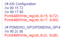
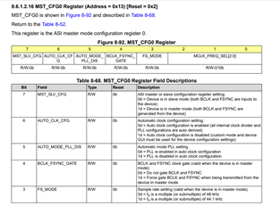
  I am using PCM6480-Q1 in slave mode,Auto clock configuration is enabled,PLL is enabled in auto clock configuration,FS is a multiple (or submultiple) of 48 kHz.

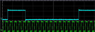
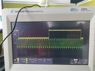
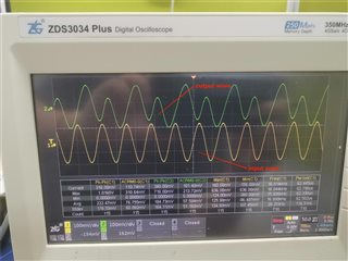
  BCLK input 24.576Mhz, FSYNC input 768Khz.

  When I input 16Khz sine wave signal to IN1, the output signal will be distorted after sampling, as you can see below:


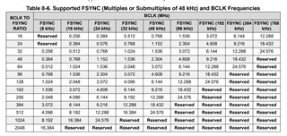
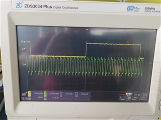
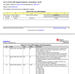
  BCLK input 12.288Mhz, FSYNC input 384Khz; or BCLK input 1.536Mhz, FSYNC input 48Khz.

  When I input 16Khz sine wave signal to IN1, the output signal after sampling is normal, as shown in the figure below:


  Please provide me some advice.

  Thanks for your help.

  • Hey Yunyun,

    Expect a response in the next 48  business hrs. 

    Regards,

    Ore. 

  • At 768Khz sampling rate, the input sine wave will produce distortion, and the higher the input frequency, the greater the distortion.

  • Hey Yunyun,

    Thanks for the details. Allow me till next week to provide feedback.

    Regards

    Ore. 

  • Hey Yunyun,

    How many output channels are you working with ? If you have enabled more than one channel, you would need to consider this formula

    BCLK= #channels* #bits per channel* sample rate frequency. 

    It would affect how your signal is sampled. If the #bits per channel is 32-bit and you have a sample rate of 768KHz, your BCLK would need to match up to that formula. So your #channels would just be one channel. 

    Hope this helps.

    Regards,

    Ore.  

  • The number of output channels working is 2, bits per channel is 16, sample rate frequency is 768Khz,BCLK input 24.576Mhz, Here is my register configuration:

    Pcm6480Write_reg(idx,0x02, 0x01);

    Pcm6480Write_reg(idx,0x07,0x40);

    Pcm6480Write_reg(idx,0x08, 0x00);

    Pcm6480Write_reg(idx,0x13, 0x27);

    Pcm6480Write_reg(idx,0x16, 0x00);

    Pcm6480Write_reg(idx,0x3B, 0xF0);

    Pcm6480Write_reg(idx,0x3C, 0x00);

    Pcm6480Write_reg(idx,0x41, 0x00);

    Pcm6480Write_reg(idx,0x46, 0x00);

    Pcm6480Write_reg(idx,0x4B, 0x00);

    Pcm6480Write_reg(idx,0x73, 0xC0);

    Pcm6480Write_reg(idx,0x74, 0xC0);

    Pcm6480Write_reg(idx,0x75, 0xE0);

    The remaining registers are configured by default, please check whether the register configuration is correct.

    Thanks for your help.

  • Hey YunYun, 

    Thanks for providing more details. While this is being reviewed, I suggest you check the register configuration for the channels in the register maps and enable and disable channels as you please. Here is an example: 


    And is your bits per channels 16-bits or is your word length 16-bits ? What ASI feature are you using TDM, I2S, or left-justified (LJ) format ?

    To check the bits per channel, use an oscope or logic analyzer to line up your fsync(frame clock) and bclk(bit clock). I have provided an example below. Here there are 16 bit clocks in one frame:

    Regards,

    Ore. 

  • Thank you for your reply,

    1.IN_CH_EN Register (Address = 0x73) ,I set the value 0xC0,Channels 1 and 2 are enabled;

    2.ASI_CFG0 Register (Address = 0x7) ,I set the value 0x40,ASI feature uses I2S mode,ASI word or slot length is 16 bits;

    3.My oscilloscope waveform is as follows:

    4.my register configuration is as follows:

    Pcm6480Write_reg(idx,0x02, 0x01);

    Pcm6480Write_reg(idx,0x07,0x40);

    Pcm6480Write_reg(idx,0x08, 0x00);

    Pcm6480Write_reg(idx,0x13, 0x27);

    Pcm6480Write_reg(idx,0x16, 0x00);

    Pcm6480Write_reg(idx,0x3B, 0xF0);

    Pcm6480Write_reg(idx,0x3C, 0x00);

    Pcm6480Write_reg(idx,0x41, 0x00);

    Pcm6480Write_reg(idx,0x46, 0x00);

    Pcm6480Write_reg(idx,0x4B, 0x00);

    Pcm6480Write_reg(idx,0x73, 0xC0);

    Pcm6480Write_reg(idx,0x74, 0xC0);

    Pcm6480Write_reg(idx,0x75, 0xE0);


    5.The PCM6480 schematic diagram is as follows:

    6.According to the datasheet,when the 768K sampling rate and BCLK TO FSYNC RATIO are 32, the BCLK frequency is 24.576Mhz;

  • Sorry, the above oscilloscope screenshot is 384K sampling rate, the following oscilloscope screenshot is 768K sampling rate:

  • Hey yunyun, 

    Thanks for the feedback, expect a response at the end of the week. 

    Regards,

    Ore. 

  • Hello,

    can you reproduce this problem on the evaluation board of PCM6480?

    thank you.

  • Thanks for your question. Expect a response in the next 48 business hours. 

    Regards,

    Ore.

  • Hey Yunyun, 

    Executing your register dumps didn't work as expected on my end. The best way to configure this device is using the ppc3 app which generated this register dump. Can you try this register dump on your end? Don't forget to use the appropriate device address when running this script. 

    I am using: single-ended inputs, 2ch, i2s mode,16bit/ch word length, 16bits/frame bclk, fs=384KHz. Try this configuration with the fs=768KHz and let me know what you find. Also, this register dump works with the mclk/fck ratio of 64 or 128 meaning my master clock is 24.5760 MHz or 49.1520 MHz respectively.

    Regards,

    Ore.

    slave mode.cfg

  • Hey yunyun, 

    any update on this ? if not I would assume this as resolved. 

    Regards,

    Ore.

  • Sorry, I have been busy with other projects recently, so this problem may need to be verified later.

  • hello,


    I have tried the register dumps you gave on my end.

    When bclk=12.288Mhz, fs=384Khz, mclk=12.288Mhz, input 10Khz sine wave signal to CH1, the output signal after sampling is normal.

    When bclk=24.576Mhz, fs=768Khz, mclk=24.576Mhz, input 10Khz sine wave signal to CH1,  the output signal will be distorted after sampling.

    I refer to the "slave mode.cfg" file and the register configuration program is as follows:

    //# Select Page 0
    //w 90 00 00
    Pcm6480Write_reg(idx,0x00, 0x00);

    //# Reset Device
    //w 90 01 01
    Pcm6480Write_reg(idx,0x01, 0x01);

    //# 1mS Delay
    sleep_ms(1);

    //# -----------------------------------------------------------------------------
    //# Begin Device Memory
    //# -----------------------------------------------------------------------------
    //# Page 0 (0x00) Dump
    //# Select Page 0
    //w 90 00 00
    //w 90 02 81
    Pcm6480Write_reg(idx,0x00, 0x00);
    Pcm6480Write_reg(idx,0x02, 0x81);

    //# 2s Delay After Disabling Sleep
    sleep_ms(2000);

    //w 90 07 40
    Pcm6480Write_reg(idx,0x07, 0x40);

    //# ASI Output CH2
    //w 90 0c 20
    Pcm6480Write_reg(idx,0x0c, 0x20);

    //# ASI Configuration
    //w 90 15 72
    //w 90 17 90
    Pcm6480Write_reg(idx,0x15, 0x72);
    Pcm6480Write_reg(idx,0x17, 0x90);

    //# PDMDIN3_GPI3/PDMDIN4_GPI4
    //w 90 2c d8
    Pcm6480Write_reg(idx,0x2c, 0xd8);

    //# Diagnostics Micbias current threshold
    //w 90 3a 10
    Pcm6480Write_reg(idx,0x3a, 0x10);

    //# Micbias Configuration
    //w 90 3b f0
    Pcm6480Write_reg(idx,0x3b, 0xf0);

    //# CH1 CFG, Gain, Volume, Gain cal, phase cal
    //w 90 3c a0
    Pcm6480Write_reg(idx,0x3c, 0xa0);

    //# CH2 CFG, Gain, Volume, Gain cal, phase cal
    //w 90 41 90
    Pcm6480Write_reg(idx,0x41, 0x90);

    //# Input Channel Enable
    //w 90 73 c0
    //w 90 74 c0
    //w 90 76 c0
    //w 90 77 f8
    Pcm6480Write_reg(idx,0x73, 0xc0);
    Pcm6480Write_reg(idx,0x74, 0xc0);
    Pcm6480Write_reg(idx,0x76, 0xc0);
    Pcm6480Write_reg(idx,0x77, 0xf8);

    //# Page 4 (0x04) Dump
    //# Select page 4
    //w 90 00 04
    Pcm6480Write_reg(idx,0x00, 0x04);

    //# High pass filter coefficients
    //w 90 49 e6
    //> 48
    //> c6
    //> 80
    //w 90 4d 19
    //> b7
    //> 3a
    //> 7f
    //w 90 51 cc
    //> 91
    //> 8b
    Pcm6480Write_reg(idx,0x49, 0xe6);
    Pcm6480Write_reg(idx,0x4A, 0x48);
    Pcm6480Write_reg(idx,0x4B, 0xc6);

    Pcm6480Write_reg(idx,0x4C, 0x80);
    Pcm6480Write_reg(idx,0x4D, 0x19);
    Pcm6480Write_reg(idx,0x4E, 0xb7);
    Pcm6480Write_reg(idx,0x4F, 0x3a);

    Pcm6480Write_reg(idx,0x50, 0x7f);
    Pcm6480Write_reg(idx,0x51, 0xcc);
    Pcm6480Write_reg(idx,0x52, 0x91);
    Pcm6480Write_reg(idx,0x53, 0x8b);

    //# Power up/down
    //# Select page 0
    //w 90 00 00
    //w 90 75 e0
    Pcm6480Write_reg(idx,0x00, 0x00);
    Pcm6480Write_reg(idx,0x75, 0xe0);

    I have some questions about the register dump,

    1.Register 0x17 does not exist in PCM6480, is it 0x16? Register 0x2C is the latched Interrupt readback register.

    2.Is mclk useful in register dump? My mclk pin uses GPIO1.

  • Hi Yunyun,

    Ore is out of office until Monday so I will address your questions in the meantime.

    1) Your correct on this. Since there is no PCM6480 EVM, Ore used a sister device in the family. These devices have register maps that are very similar, but that discrepancy was overlooked. If they don't belong to the 6480 register map, I would disregard those lines.

    2) I'm not sure what you mean by useful in the register dump, but you are right to have MCLK on GPIO1 if you are using Master Mode. From your schematic it looks like you're in slave mode? i.e. BCLK and WCLK are being provided by a host? In slave mode MCLK isn't necessary since BCLK can be used as a PLL source.

    Best regards,
    Jeff McPherson

  • hello
    I'm using slave mode, and BCLK/WCLK/MCLK are all provided by the FPGA.

    In the "slave mode.cfg" file, I see the Settings for mclk, but mclk should not be in effect.

    //# ASI Configuration
    //w 90 15 72
    //w 90 17 90
    Pcm6480Write_reg(idx,0x15, 0x72);
    Pcm6480Write_reg(idx,0x17, 0x90);

    According to the "slave mode.cfg" file, In register 0x13, PLL is enabled in auto clock configuration(AUTO_MODE_PLL_DIS = 0), But in register 0x16, Bit 7 is set to 1, which I think is invalid, because Audio root clock source setting when the device is configured with the PLL disabled in the auto clock configuration for slave mode (AUTO_MODE_PLL_DIS = 1).

    So, what is the clock source when the device is configured with the PLL enabled in the auto clock configuration for slave mode (AUTO_MODE_PLL_DIS = 0)?

  • Hi Yunyun,

    You are correct that register 0x16 bit 7 will be ignored as long as the auto clock configuration mode is active. The clock source in automatic mode is BCLK. The PLL and dividers use this as the clock source to create all other clocks.

    Best regards,
    Jeff McPherson