This thread has been locked.

If you have a related question, please click the "Ask a related question" button in the top right corner. The newly created question will be automatically linked to this question.

TLV320AIC1110: DVDD and AVDD of the TLV320AIC1110

Guru 12235 points
Part Number: TLV320AIC1110
Other Parts Discussed in Thread: TLV320AIC1103

Hi,

I have two questions about the power supply of the TLV320AIC1110.

Q1.
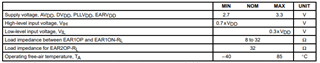
Is it OK as long as VDD adheres to the rated 2.7V~3.3V? In other words, does VDD need to be 3.0 V?

Q2
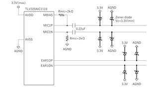
Is there any problem with the analogue power supply (AVDD, EARVDD) being separated from the digital power supply (DVDD, PLLVDD) by a coil and connected?
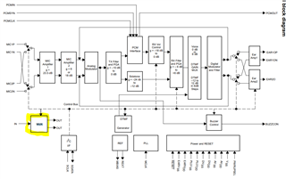
In slau090, p.22, it was connected to 3.3V_A via FB5 from DSP_3.3VDC, which is separate from 3.3V_D. Do 3.3V_D and 3.3V_A need to be completely separated?

Thanks,

Conor

  • Hi Conor,

    Yes, as long as VDD is between 2.7V and 3.3V the part will work as described. VDD does not have to be exactly 3V.

    I don't see the example you're referring to in https://www.ti.com/lit/pdf/slau090 but generally it's better to separate analog and digital power supplies for noise coupling reasons. However this is not a requirement for this part.

    Best regards,
    Jeff McPherson

  • I understand the power supply range.
    I would like to know about the circuit configuration of TLV320AIC1110 additionally.

    Q1.
    What is the role of the capacitor (Ci) connected to MIC1N and MIC1P?

    Q2.
    In the "TLV320AIC1103/1109/1110 EVMs User's Guide", the 1206 size is used, but is the larger size better? Is there any problem with the 0603 size if other specifications such as capacity are the same?

    Q3.
    In the circuit below, MIC1P is connected to GND via Rmic. Is there any problem if MIC1N is connected to GND?

    Thanks, 

    Conor

  • Hi Conor,

    Ci is a input coupling capacitor. Its purpose is to remove DC offset from the input signal, including MBIAS

    We have an app note that explains what to consider when choosing coupling capacitors: https://www.ti.com/lit/an/slyt796a/slyt796a.pdf?ts=1693927774082&ref_url=https%253A%252F%252Fwww.google.com%252F

    Did you mean to ask if MIC1P is connected to GND? MIC1P is tied to GND through Rmic so that the impedance is balanced on both the positive and negative side of the mic terminals. If you mean to tie MIC1N to GND as an unused input, that is fine as long as Ci is in series with GND.

    Best regards,
    Jeff McPherson

  • Hi Jeff

    We have an app note that explains what to consider when choosing coupling

    What are the concerns about changing from size 1206 to 0603?

    Did you mean to ask if MIC1P is connected to GND?

    In the datasheet it is the 'P side' of MIC1, but is it problematic to connect the 'N side' of MIC1 to GND via Rmic?

    Q4.
    The "overload signal level" listed on page 14 of the datasheet is 4.54Vpp at 32-Ω load RXPGA = -4 dB. In the "Absolute Maximum Ratings..." section, Vo is listed as -0.5V to 3.6V, which seems to indicate that the output exceeds the absolute maximum ratings. What does the voltage listed for the overload signal levels mean? My understanding is that it means the voltage between EAR1OP and EAR1ON is 4.54Vpp.

    Thanks,

    Conor

  • If all else is equal then there is no concern between 1206 and 0603. As the app note explains, the risk comes more into play with the dielectric used.

    Since the amplifier is differential, then there is no issue connecting N side of MIC1 to GND via Rmic.

    According to NOTE 10 on page 14, these voltages are measured differentially between EARON and EAROP so your understanding is right. The Absolute Maximums are measured with respect to GND. On each individual pin, the voltage is ~2.25Vpp which still satisfies the absolute maximum.

    Best regards,
    Jeff McPherson

  • Hi Jeff, 

    If all else is equal then there is no concern between 1206 and 0603. As the app note explains, the risk comes more into play with the dielectric used.

    Ci will use Samsung's CL10B224KO8NNPC (0.22 uF); according to the data sheet for the CL10B224KO8NNPC, the application of a 2.5 V DC voltage causes a capacitance drop of approximately 50%. If the effective capacitance drop due to the DC bias characteristic is large, this may affect the removal of the DC offset from the input signal. Can you comment on something?

    Since the amplifier is differential, then there is no issue connecting N side of MIC1 to GND via Rmic.

    There is no functional difference between connecting MIC1N to GND and MIC1P to GND, is there? If MIC1N is connected to GND, then MBIAS is connected to the MIC1P, correct?

    Thanks,

    Conor

  • Hi Conor,

    The capacitors only purpose here is to absorb the DC offset. The capacitor will form a high pass filter with the input impedance. The fully differential impedance is 60kOhm so each side sees 30kOhm. With a 0.22uF coupling cap, this has a cut off of 24Hz which is pretty normal considering the audio band starts at 20Hz. If the capacitance were to drop to 0.11uF the cut off raises to 48Hz. 

    As long as the capacitor forms a desired high pass filter while the 2.5V MICBIAS is applied, then there is nothing to worry about.

    For your second question, yes. The amp is differential so the only consequence is a 180 degree phase shift.

    Best regards,
    Jeff McPherson

  • Hi Jeff,

    Thanks for the reply. I would like to ask one additional question. The TLV320AIC1110 has two selectable MCLK clocks (128 MHz or 2.048 MHz) as follows. How are these clocks used differently?

    Thanks,

    Conor

  • Hi Conor,

    It's my understanding that these clocks come from older PCM conventions. Both clocks are supported as inputs to the device, the difference is the clock processing. It won't result in any meaningfully different power consumption, they are just different options to support clock flexibility.

    Best regards,
    Jeff McPherson

  • Hi Jeff,

    The capacitors only purpose here is to absorb the DC offset. The capacitor will form a high pass filter with the input impedance. The fully differential impedance is 60kOhm so each side sees 30kOhm. With a 0.22uF coupling cap, this has a cut off of 24Hz which is pretty normal considering the audio band starts at 20Hz. If the capacitance were to drop to 0.11uF the cut off raises to 48Hz. 

    1. What value should I use as a guide for the cut-off frequency? The audio bandwidth is 20Hz~, but even without considering DC bias, it is a little over at 24Hz with 0.22uF in the reference circuit.

    2. There is no information on Rmic in the datasheet except for Figure 12: Rmic is pulled up on MBIAS and pulled down on GND for the inputs of the differential amplifier, can you tell us what it is used for?

    Thanks,

    Conor

  • Hi Conor,

    1) It's a trade off between your application requirements and your costs. 0.22uF is a very common capacitor value and a low power device like this typically isn't driving a speaker that can support a frequency as low as 24Hz anyway. If that low end of the spectrum is important to your application then you will need to raise the capacitance value to 0.47uF for example.

    2) The Rmic are pull up/down resistors for the mic, not the amplifier. The coupling capacitors separate the two. The Rmic to MICBIAS is to power the microphone. The Rmic to GND is because a differential mic will typically bias both sides so that they match in amplitude. This resistor value is typically the same output impedance of the microphone in order to maximize power delivery. 2.2kOhm is a common choice for this bias resistors.

    Best regards,
    Jeff McPherson

  • Hi Jeff,

    Thank you always for your help.

    Q1.

    0.22uF is a very common capacitor value and a low power device like this typically isn't driving a speaker that can support a frequency as low as 24Hz anyway.

    The data sheet contained the following information.

    ----------------------------
    A low-pass filter attenuates the signals over 4 kHz. A selectable high-pass filter cleans up the signals under 100 Hz. This reduces noise that may have coupled in from 50/60-Hz power cables. The high-pass filter is bypassed by selecting the corresponding register bit.
    ----------------------------
    When using a high pass filter by register setting, There is a description that it removes signals below 100Hz. In that case, is a capacitor that filters frequencies below about 20Hz unnecessary? Or even if I set up a resistor, do I still need to place a capacitor?

    Q2. 

    The Rmic to MICBIAS is to power the microphone.

    Is it correct to understand that the meaning of the above is to propagate the waveform above 0V by adding the Bias voltage as shown in the figure below?

    Thanks,

    Conor

  • Hi Conor,

    Q1) From a filtering point of view, yes the filter is unnecessary since the digital filters will take care of it. However that capacitor is relevant to Q2

    Q2) You are correct, the effect of the bias will be that the signal raises above 0V. That's why the coupling capacitor is important, so that the signal returns to 0V.

    Best regards,
    Jeff McPherson

  • Hi Jeff,

    Q1.
    What is the MUX (analog switch) of TLV320AIC1110 used for? Is it okay to leave unused processing open?

    Q2.
    If MIC2 input is not used, should I connect it to GND on the analog side? Or is it okay to open it?

    Thanks,

    Conor

  • Hi Conor,

    1) Can you be more specific? Pin# or Register#? I'm not sure which MUX you are referring to.

    2) Unused MIC inputs are recommended to be AC coupled to GND via 0.47uF or similarly sized capacitor due to noise performance reasons. If noise performance is not a major concern, the unused MIC inputs can be disconnected from the PGA using settings in Page 1 Register 48 and the pin can be left floating.

    Thanks,
    Jeff McPherson 

  • Hi Jeff,

    1) Can you be more specific? Pin# or Register#? I'm not sure which MUX you are referring to.

    Sorry, MUX meant the following. I would like to know about the intended use and how to handle of unused pin.

    Thanks,

    Conor

  • Hi Conor,

    Thank you for the clarification. It's an analog mux to allow an analog input signal to pass through to different loads. If it's unused I would ground the input pin and leave the outputs floating.

    Best regards,
    Jeff McPherson

  • Hi Jeff,

    Q1.
    I am considering mounting an external zener diode for overvoltage protection on the analogue inputs and outputs (MIC1P/N, EAR1OP/N) of the TLV320AIC1110, I plan to use a component with Vz=3.3V (min), is this a problem?

    Q2.
    Is it OK if PCMCLK and MCLK are asynchronous?

    Q3.
    PLL once in FPGA from oscillator, generate 2.048MHz and input to MLCK of TLV320AIC1110 There is PLL processing in TLV320AIC1110, but is there any problem if PLL is multi-staged?

    Q4.
    In Data Sheet Figure 1 and Figure 2, is there any problem with PCMCLK continuing to be output before 0 and after N+1?

    Q5.
    Is it correct to understand that the PCMO goes Hi-Z at a minimum of 30ns after the falling edge of the Nth bit clock, as in tpd3 in Figure 1?

    The following statement is found in the power-on initialisation section of the data sheet.
    'In addition to resetting the power down bit in the power control register, loss of MCLK (no transition detected)
    automatically enters the device into a power-down state with PCMO in a high impedance state."
    Will the PCMO be Hi-Z in states other than the power-down state described above?

    Thanks,

    Conor

  • Hi Conor,

    1) Yes this is fine,

    2) PCMCLK and MCLK must be synchronous

    3) There should be no issue as long as you are sending the correct 2.048MHz clock to the codec.

    4) PCMCLK should run continuously. 0 and N+1 are just markers to show how the MSB and LSB aligns within the transmit time slot.

    5) Yes you are correct. Without a subsequent PCMSYNC trigger the output will go to high-z

    Best regards,
    Jeff McPherson