This thread has been locked.

If you have a related question, please click the "Ask a related question" button in the top right corner. The newly created question will be automatically linked to this question.

OPA1637: OPA1637 pspice model

Part Number: OPA1637
Other Parts Discussed in Thread: THS4551, THS4521

hi 

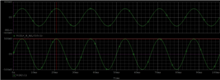
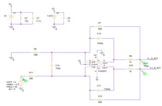
i am simulating OPA1637 pspice model for my application (current _sensing for DC charging stataion)and facing difficulty in determining how to accurately input the corrent voltage to Vocm pin 

under my understanding , i assumed that output waveform should be offset by voltage (1.65V) applied to Vocm pin,however,the simulation results are not alingning with this assumption.

Therefore, I have the following questions:

1. is my simulation circuit  correct ?

2.could you provide guidance in the proper method  or voltage level to apply as an input to the Vocm pin? 

3.is OPA1637 suitable choice for my applicaiton or would you recommend an alternative?

  • (IL-_R_AD and IL+_R_AD) is output waveform

  • Hi Ethan,

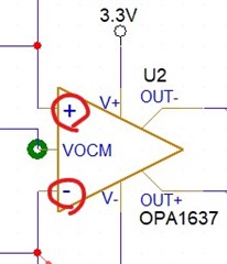
    The OPA1637 needs at least 1 V input common-mode above the negative supply voltage to work correctly.

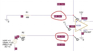
    In your configuration, you are setting the output common-mode voltage to 1.65.  The input signal is ground referenced, so the input common-mode voltage that the device sees is calculated from the resistor divider of R1 (or R2) and R3 (or R4), meaning that when the input voltage is zero, both legs of the output should sit at 1.65 V, and the input singal (meaning the input where V3 is connected) is at 0V. Then the voltage at the inputs of the OPA1637  = 1.65*499*/(698+499) = 0.68 V.  Unfortunately the OPA1637 cannot be used in this case.  You would either need to raise the output common-mode voltage to ~2.43 V, or pick another device.

    THS4551 can work for this case, it has an input common-mode voltage down to Vs- - 0.1 V.  

    Regards,
    Mike

  • HI Michael

    thanks your answer 

    i still am confused with following question 

    1. I try to simulate other pspice (OPA1637 ,THS4551,THS4521), whatever Vocm is . i found the output waveform fails  and no offset voltage.
    2. could you provide guidance in the proper method  or voltage level to apply as an input to the Vocm pin? or TI Pspice model dose not support this function?

    thanks in advance 

  • Hey Ethan, 

    Can you attach your Pspice simulation for us to take a look at?

    For a quick reference using Tina Ti and our reference design circuit, you can see that with a voltage applied at Vocm of 2.5 V, the output common mode voltage is roughly 2.5 V. This value can be adjusted by changing the voltage source below that is jumpered to the Vocm pin. The Vocm voltage must be within the min and max values Mike highlighted above for linear operation of the device. If you provide your Pspice simulation I can demonstrate the behavior below. There is an attachments option when you reply that can be used to attach your simulation. 

    Best Regards, 

    Chris Featherstone

  • hi chris 

    i attach a Pspice file and i still do not understans why OPA1637 cannot meet our design but THS4551 can OPA1637DGKR_TI.DSN

  • Hey Ethan, 

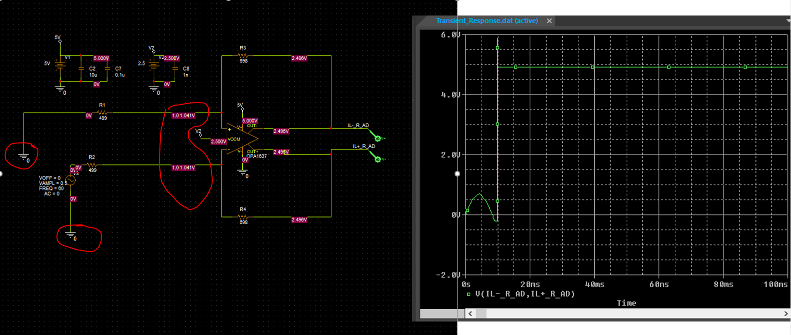
    It looks like the issue is that the supply is single sided and that the input signal is relative to ground. You can see that the input pins are sitting at approximately 1V and this means that the DC common mode is at approximately 1V above the negative supply which is ground. This is the minimum allowable input common mode range that will allow the device to operate within the linear region. The issue arises when the input AC signal is taken into account. The moving AC signal is relative to ground and causing the input common mode range to be violated. Below you can see that the transient analysis shows the output railed out. I fix this in the next image below. 

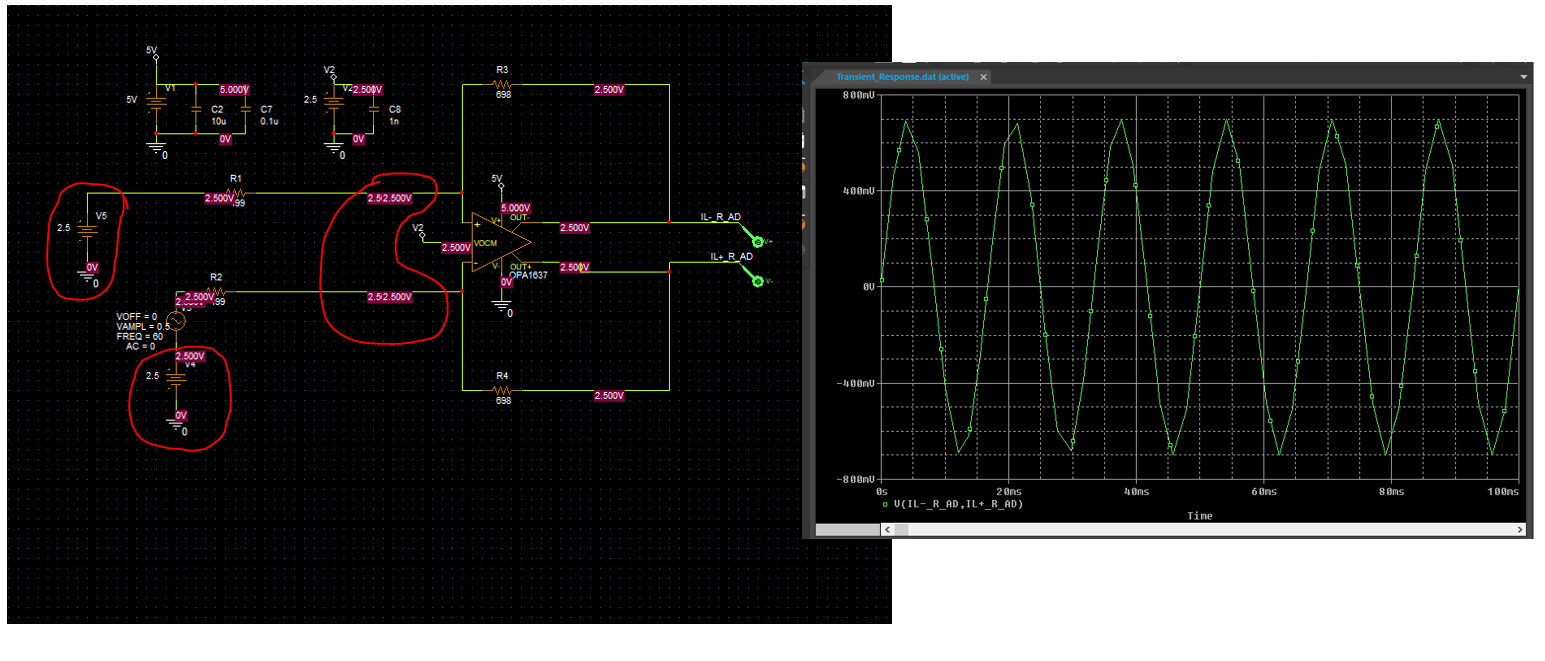
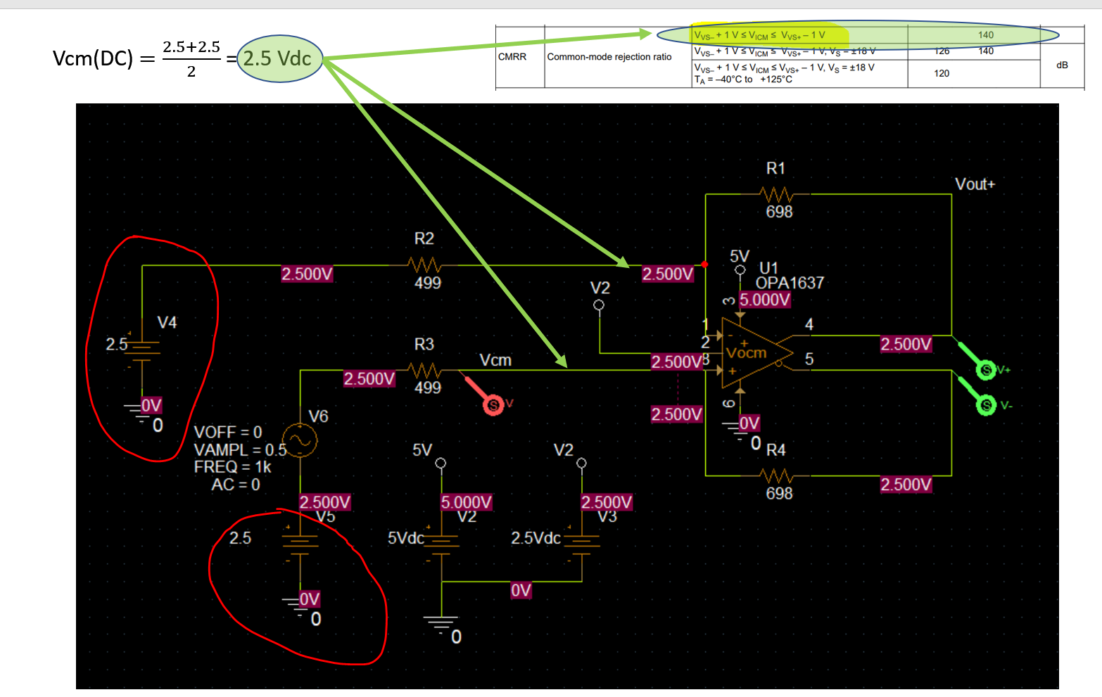
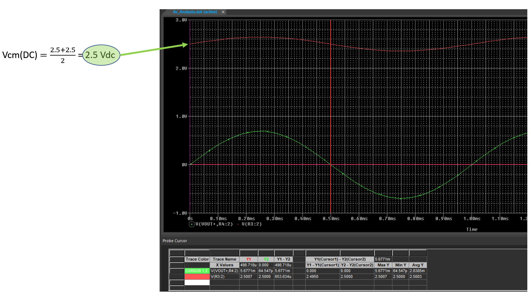
    Below you can see that the DC input common mode voltage is now 2.5V above the negative supply that is at ground. In addition the input AC signal is relative to 2.5V DC as well. The device is operating within the linear operating range and we get the signal on the output. 

    Here is my updated Pspice simulation. I hope this helps answer why the OPA1637 wasn't providing the expected results in PSpice. Let me know if you have any further questions. 

    OPA1637DGKR_TI-PSpiceFiles.zip

    Best Regards, 

    Chris Featherstone

  • Hi Chris

    thanks your feedack 

    i have two topics to be updated 

    1. update my pspcice design 

    i studied an training video from TI

    https://www.ti.com/video/series/precision-labs/ti-precision-labs-ti-pl-amps-fully-differential-amplifiers.html

    i thought  the input+ /  input- voltage to OPA1637  dose not meet its specification so that outpout voltage is not corrent.


    therefore . i design new AV (only for testing) and a result is in my expectation.   do you think it is main issue at my design?

    2.your pspice design 

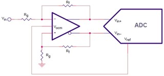
    in my understand , the signal-end in to diff-out  is similar to picture . so i cannot understand why input+ need an offset voltage ? from your simulation , it appears that the output voltage dose not depends on the offset voltage for swinging 

    thnaks you in advance 

  • Hey Ethan, 

    We are currently looking into your question and will respond within one business day. 

    Best Regards, 

    Chris Featherstone

  • Hey Ethan, 

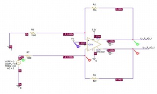
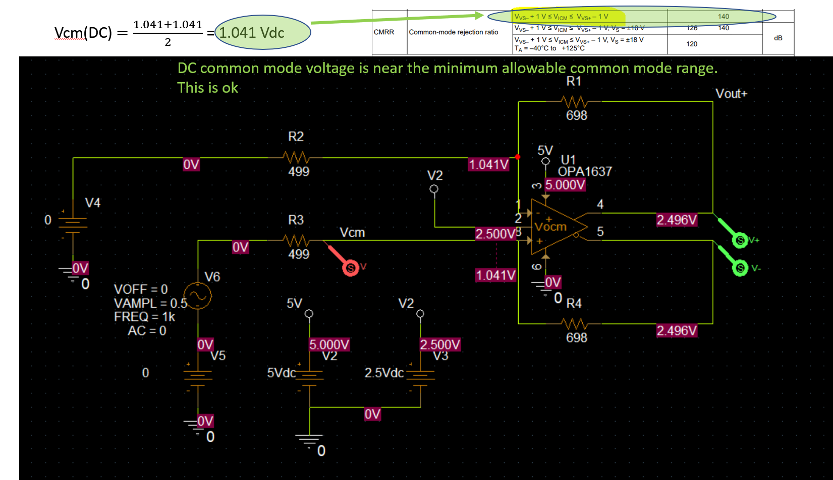
    The DC common mode voltage of 1.041V is within the linear operating range. The common mode voltage is being violated when the AC signal is applied. I created some illustrations below that I hope will help clarify the issue. 

    The DC common mode voltage is ok here:

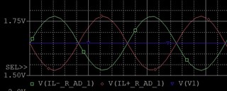
    Here is where the issue occurs. You can see below that the output voltage is clipped when the common mode voltage falls below 1V. In this region the amplifier is no longer in the linear operating region of operation. 

    Therefore the DC common mode voltage needs to be shifted up such that when the AC signal is applied to the input, the common mode voltage stays within the linear operating range. 

    After shifting the DC common mode voltage to mid-supply the amplifier now operates within the linear operating range when the AC signal is applied. 

    I hope this helps clarify the issue. Let me know if you have any further questions. 

    Best Regards, 

    Chris Featherstone

  • hi Chris

    thank for your feedback

    I have one more question

    Q1:How to measure dB and Phase Margin at differential signal?

    DB(V(IL+_R_AD_2)) - DB(V(IL-_R_AD_2)) is my idea but the waveform seems to look not correct 

         thanks in advance 

  • Hey Ethan, 

    We have a training series here that demonstrates how to do stability analysis for fully differential amplifiers in simulation. 

    https://www.ti.com/video/series/precision-labs/ti-precision-labs-ti-pl-amps-fully-differential-amplifiers.html

    Let me know if I can be of further assistance. 

    Best Regards, 

    Chris Featherstone