Could you please help with below queries:
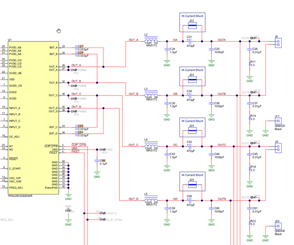
1.The TPA3250 has some short detection and protection of the outputs to ground. How does this work in combination with the 470uF in series? With the 470uF in series, DC on the output can be prevented.
2.Selection of R11 resistor Resistor power ratting for 60 and 120W application.
C26+R11 is used as an load of the class D filter when the loudspeaker load is higher than 120W. This circuit dampens the resonance of the filter around the cut-off frequency.
How is overloading, overheating and breakdown of the 0.5W resistor prevented when the amplifier is driven with high frequency signals in an unloaded condition?
3. whether a high resistive path (e.g. 47k) on both sides of the capacitor to a defined DC value (e.g. GND and a small DC level) is required?
a: For the leakage current of the elcap C21, C34, C42, C56) preventing DC voltage creation on the primary side of the transformer.
b: The elcaps need a (small) DC voltage during usage.
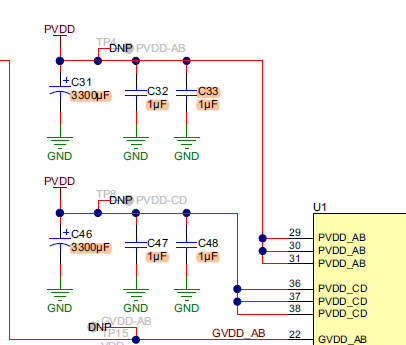
4.Why supply for the TPA3250EVM board divided over two circuits? L1 and L2.