Other Parts Discussed in Thread: PCM1794A
Hello Mr or Mrs.
Happy new year~!I am always grateful for your help. :)
I am designing a circuit which is related DAC output and it confuses me.
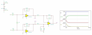
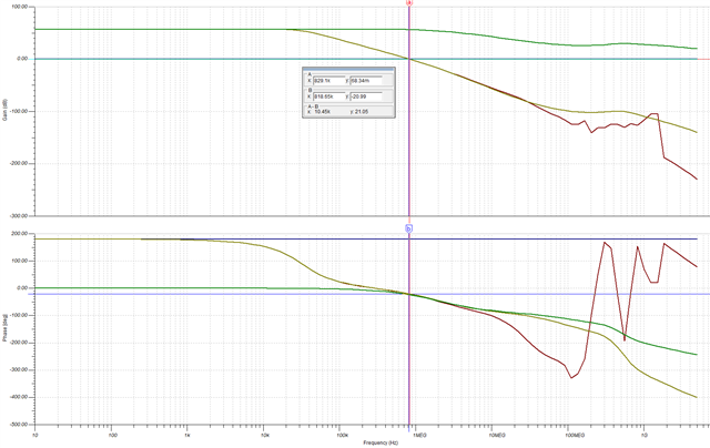
This is a PCM1794a reference TINA simulation design and bode plot.
It looks two stages that first I/V conversion and filter with summation.
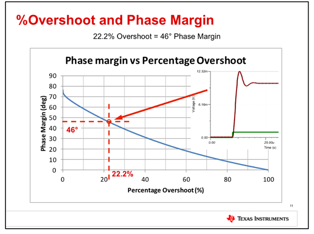
I heard lack of phase margin can cause oscillating problem thus over 45 deg of phase margin is required.
In the reference simulation, however, it looks lack of phase margin.(3 deg?)
The reason why I ask you this question is that I am struggling for phase margin.
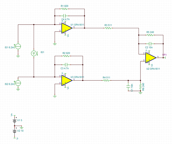
This is my simulation design.
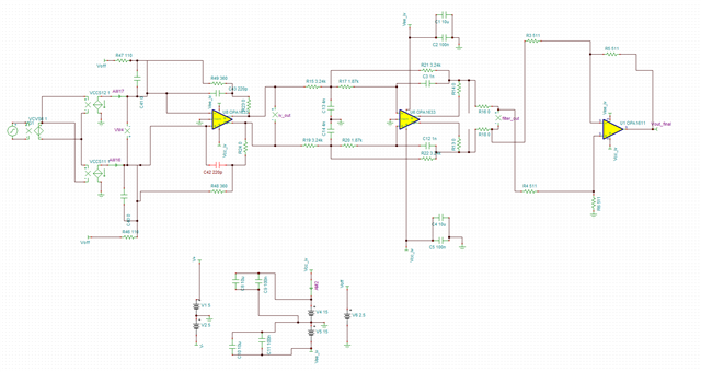
DAC output current: +- 18.2mA
Filter topology: MFB (fc: 32140Hz) - TI filter pro 2nd LPF and mirror for FDA.
Vcc Vee: +-15V
INPUT: Sine wave generator.
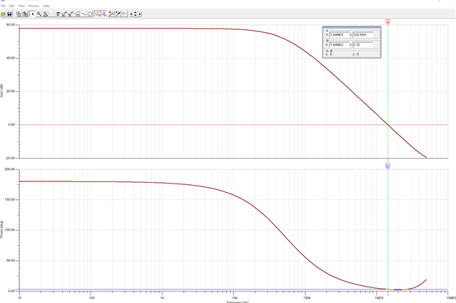
After LPF stage, It looses phase margin(Actually unstable).
I just wonder....
1. I don't have to worry about the point where the gain is 0db outside the frequency range I'm interested in(10 ~ 22kHz)
2. Should input and output be considered for each stage? ( Input vs output of I/V, LPF, or Balanced to Single stage)
3. My circuit design is wrong...
I attached TSC file.
Please give me a advice.