This thread has been locked.

If you have a related question, please click the "Ask a related question" button in the top right corner. The newly created question will be automatically linked to this question.

PCM5102A: DAC output

Part Number: PCM5102A

Hi,

We are using PCM5102A in 4-wire I2S mode for Non -audio frequencies. All the clocks (SCK,LRCK,BCK) and DIN are generating from FPGA and feeding to DAC. 

We tried this circuit for common audio frequencies aswell. But the DAC output is not coming even for 32KHz. Herewith attached the schematics for your reference. Please review and let me know your comments. I am listing the below observations when we tested the circuit. VNEG voltage is coming as 0V, What will be the reason for that? Will this affect the DAC out?

1. LDO voltage is coming as 1.92V

2. VNEG voltage is observing as 0V.

3. No voltage can be observed across CAPP and CAPM.

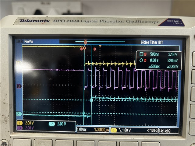
4. I2S plots are as expected in FIG 14 datasheet. Attached snapshots. 

With regards,

Sujisha V
  • Hello Sujisha,

    Clearly the negative charge pump is not working and that will lead to a non functioning DAC. For charge pump to work correctly, it needs the correct clocking as well as correct flying capacitor and input .

    So to find the root cause of this issue would you please try to make sure the following have the correct capacitors ( and correct polarity)

    CAPM , CAPP ,  CPGND  CPVDD and VNEG. Please refer to Figure 5. PCM510xEVM-U Schematic in the user's guide for reference 

    once these are verified, the only possible item on the list is the clks, Since we do not have access to internal clks, we have to make sure the issue is there even for nominal clks,

    Which means we have to try it with an audio sampling frequency such as 48K with whatever bit depth you are using.  The device accepts 16-, 24-, and 32-Bit Audio Data

    So lets say you are sending 32 bit data,  then the BCK would be 2x32x48KHz.

    SCK should be a multiple of LRCLK , you can try 64x48KHz or 128x48KHz   or 256xfs  but up to Up to 50 MHz for your SCLK. ( refer to Table 2. PCM510xA Audio Data Formats, Bit Depths and Clock Rates) 

    Please confirm the operation  with these steps in mind and let me know what you find out.

    Regards,

    Arash

  • Hi Arash,

     * We verified the capacitors on VNEG(2.2uF Ceramic),CAPP,CAPM(2.2uF Ceramic) and CPVDD(1uF,10uF ceramic). All these rails are provided with correct capacitor as per the EVM schematics and no capacitor damage can be seen on the board.

    * We tried with 32KHz audio frequency with 32bit. The below frequencies are generating from FPGA. 

    SCK= 128Fs = 4.096MHz

    BCK = 64Fs = 2.048MHz

    LRCK = 32KHz (LRCK divider =128)

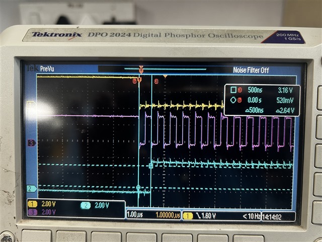
    While probing, all these frequencies are coming correct and timing also proper only. Attached the image for reference. In the image, 

    Yellow - LRCK,  Pink - BCK, Blue - Data Input

    Please let me know your comments from these observations.

    with regards,

    Sujisha V

  • In addition to above observations, 

    Today we observed -3.3V on VNEG and across CAPP and CAPM after programming. 

    Without programming no voltage can be seen on VNEG and CAPP& CAPM. Is this correct? Is this Charge pump work only after programming ? Then what will be the pin status for VNEG, CAPP,CAPM default condition when power on?

    If the charge pump works only after programming and we are able to get proper voltage and clocks , then what will be the issue with DAC output?

    with regards,

    Sujisha V

  • Hello Sujisha,

    If you are using PCM510xA , it doesn't have any I2C pin to program and I don't recall I have ever used it in anything except HW mode.- I just provided I2S (clks and  digital input), power it up  using USB and that was all I had to do. The reconstructed sine wave was at the output pins.

    Section 7 Pin Configuration and Functions of datasheet shows no I2C pin for programing. In fact datasheet emphasis on Simple Configuration Using Hardware Pins

    You are using your own generic PCB, without any SRC part which needs programing, So I am not sure i understand the programming part for the DAC.


    Can you please confirm what you mean by programming the part?  And how you programed the DAC? 

    Regards,

    Arash

  • Hi Arash,

    Sorry for the incomplete explanation. We are using PCM5102A and that has only HW mode. Programming means once I program the FPGA for generating Clocks and Data input, then only the charge pump is working and we are observing -3.3v on VNEG and across CAPP and CAPM. 

    With power on, without feeding these clocks , charge pump is not working and no voltage can be seen on the charge pump related pins. Please let me know whether charge pump can work in default power on condition without feeding any clocks and data.

    If charge pump can only work with feeding clocks and we are able to get all the voltages, what will be the other issues with DAC output? Please reply ASAP since we are in a critical situation.

    with regards,

    Sujisha V

  • Hello Sujisha,

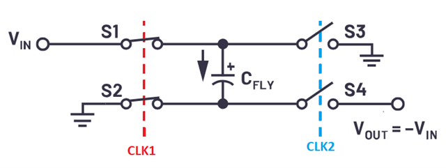
    As I showed you in the simple drawing of the charge pump, it needs two phase clock to generate the negative voltage so if the clks are not provided then the charge pump should not work. 

    If all voltages are correct at the pins of the IC then it has to be something with the clks or format of data. I can not think of anything else.

    The only thing that I can think of is to use a different source for generating your clks to verify there is any issue with the clocks. This is a very simple part and you already verified the voltages and supplies. If it is not muted, it has to be the I2S issue.

    Regards,

    Arash