This thread has been locked.

If you have a related question, please click the "Ask a related question" button in the top right corner. The newly created question will be automatically linked to this question.

OPA1679-Q1: About thermal pad

Part Number: OPA1679-Q1
Other Parts Discussed in Thread: OPA1679

Hi team,

In OPA1679-Q1 datasheet, there are no specification for the thermal pad connection. So, my customer has connected the thermal pad to GND.
But in OPA1679 datasheet, it says that the thermal pad should be connected to V-. Also, it is explained in the related thread too.

Just too double check, the customer should not connect the thermal pad to GND, right? If so, could you update the datasheet for OPA1679-Q1 and write that the pad should be connected to V-?

Regards
Ohashi

  • HI Ryoma,

    Yes, the OPA1679 datasheet recommends to connect the thermal pad to the most negative supply V-. The thermal pad must be soldered to improve heat dissipation and provide specified performance. This is also true for the OPA1679-Q1.

    I have provided the feedback/ filled the form to the systems team and this should be in the queue for the next datasheet revision.

    Thank you and Regards,

    Luis

  • Hi Luis.

    Thanks for your support. Got it that thermal pad has to be connected to V-.

    The customer wants to know the potentail issue that might happen by connecting the thermal pad to GND. The already have built the 1st proto with the thermal pad connected to GND. The will plan to change this in the 2nd proto, but wants to continue the evaluation with thermal pad connected to GND for the 1st proto.

    So, my customer wants to know what might happen by connecting the thermal pad to GND.

    Regards,
    Ohashi

  • HI Ohashi-san,

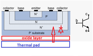
    The thermal pad must be connected to the most negative supply Vs-.  The thermal pad needs to be connected to the most negative supply and not other potential to ensure proper performance.  Almost all modern semiconductor products use p-substrate process to implement the transistor-level circuitry, which require the p-substrate to be biased at the most negative supply voltage used to power the IC. Thus, connecting the thermal pad (located at the back-side of the silicon wafer) to any voltage above (V-) may result in current leakage that increases at the elevated temperature – see image below.

    Thank you and Regards,

    Luis