


Hello TI,
1. We have a requirement to (non-concurrently) support two full-scale modes: 1 Vrms [around 1.65 VDC common mode] (line 1 in the table below) as well as 0.5 Vrms [around 0.9 VDC common mode] (line 3 in the table below).
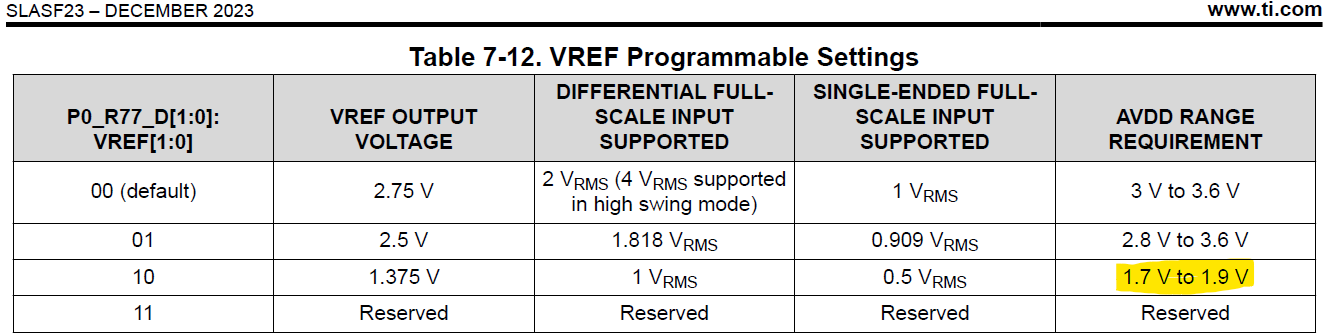
We assume that an internal LDO generates Vref from AVDD. Question: Is the "1.7 V to 1.9 V" in the table above a hard requirement, or would it be possible to generate Vref = 1.375 V from an AVDD of 3.1V? i.e. Is it possible to supply AVDD=3.1 V to the part and still support 0.5 Vrms full-scale input swing around 0.9 VDC (similar to DAC side of TLV320AIC32x4 / TLV320AIC32x6)?
2. Similar to above, but on output / DAC side: Is it possible to supply AVDD=3.1 V to the part and still support 0.5 Vrms full-scale output swing around 0.9 VDC (similar to TLV320AIC32x4 / TLV320AIC32x6)?
3.When is the next update of the datasheet expected?
