This thread has been locked.

If you have a related question, please click the "Ask a related question" button in the top right corner. The newly created question will be automatically linked to this question.

PCM3060: About analog input (input impedance) block diagram

Part Number: PCM3060
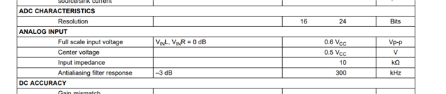
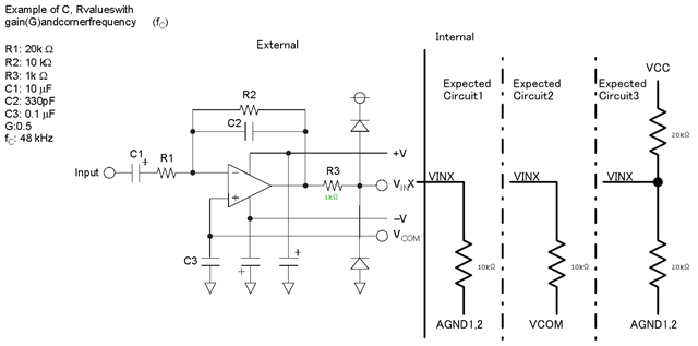
I would like to see a block diagram of the analog input circuit.
The figure below shows the expected circuit of the internal block.
If it is expected circuit 1, an ADC input will be offset to the negative side. I think it is not expected circuit 1.


Regards,
Hiroshi.
  • The centre voltage for the ADC is 0.5*Vcc as is indicated in the chart above,

    Also Vcom=0.5*Vcc. For Vcc of 5V , Vcom=2.5V dc.

    In the Schematic the positive input pin of the OP Amp is fixed to 2.5v. The DC Feedback shall set the OP Amp output as well as ADC Input to 2.5V DC which is the centre value. An AC Signal of 3vpp at OP Amp output takes the  ADC input to a Max level of 4v and a Min level of 1V

  • When simulating the recommended circuit in the data sheet, the output is saturated at an input of 2Vrms.

    This is due to the level shift caused by the 1kΩ and 10kΩ voltage divider circuit.
    What is this 1kΩ recommended for? 

  • From a signal point of view the 1k is not needed.

    It might however be that at t=0+ when the input capacitors are a short then the output of the op amp may go +V. The external 1K may limit the current going into the protection diodes. Such a situation may also happen with an input signal which is very large.

    Normally if the Vcc of the external op amp is 5V and the ADC Vcc is also 5 v then the protection diodes shall never fire. In this case the 1k can be made a 47 ohm