This thread has been locked.

If you have a related question, please click the "Ask a related question" button in the top right corner. The newly created question will be automatically linked to this question.

PCM3060: How to properly bias inputs

Part Number: PCM3060

Hi there,

I'm seeing some conflicting information in the PCM3060 datasheet and here on the forum that has me confused about how to properly connect a buffered AC signal to the PCM3060 input.

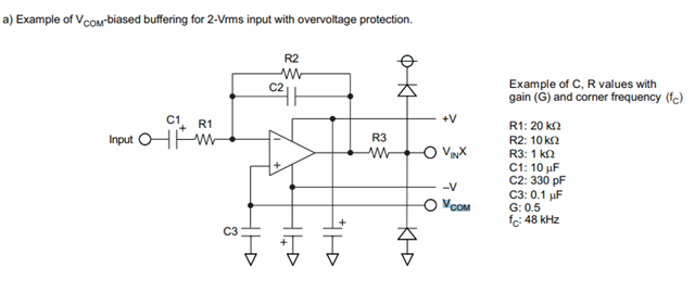
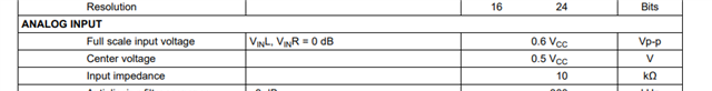
First, the application example circuit in the datasheet recommends we connect Vcom to the + pin of an op amp. Vcom is supposedly 0.5* Vcc. If Vcc is 5V then this would result in a 3.75V offset applied to the input of the ADC (VinX). If the full scale input range is about 0V to 5V, then why 3.75V?

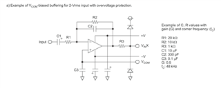
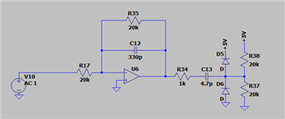
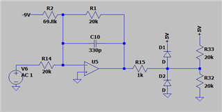
In-addition, one page earlier, the typical connection diagram recommends using a large bypass capacitor at the input, which isn't shown in the application example above. Why would we use Vcom to bias the input up to 3.75V if we're just going to remove it with the bypass capacitor?

Furthermore, this post here on the forum (https://e2e.ti.com/support/audio-group/audio/f/audio-forum/1236805/pcm3060-ac-couple-analog-inputs?tisearch=e2e-sitesearch&keymatch=PCM3060#) states that you don't need to bias the input at all and the input circuitry provides the 2.5V bias required. So why does the application circuitry recommend using Vcom?

  • Here is what I'm assuming is going on - and I'm wondering if someone can correct me if I'm wrong:

    1. The internal bias is very "weak" and is made up of something like a pair of 20k bias resistors (hence the 10k input impedance). Without the biasing, we need the bypass capacitor (like below), otherwise the output impedance of the op amp will drag the bias down.


    2. If we use external biasing, we no longer need the large electrolytic bypass capacitor. The recommended circuit works but it is not ideal - it doesn't quite get the offset voltage into the exact position for full scale input swing but it is OK enough.

    A better circuit (below), which biases the input precisely at 2.5V might be a better option to get the most headroom. Correct?


  • I shall respond in a few hours

  • In the application circuit Vcom of 2.5v DC on Positive pin of op amp results in 2.5v DC on input pin when there is no signal present. This is the DC Condition of the circuit. Vcom=0.5*Vcc. If Vcc =5V Vcom=2.5v

    The circuit has a Gain of 0.5 So a 2V RMS input signal shall result in a 1V rms signal riding on the 2.5V Bias giving a 3VPP Signal into the ADC.

    This satisfies the datasheet spec

  • Ah! I think I discovered my confusion. The presence of C1 blocks the DC from the input circuit so the Vcom is not affected by the gain of the op amp. Without C1, the offset is 3.75V. But with C1, the offset is as expected. Thank you for clearing that up.

    I will still use a different approach so that I don't have to use C1.

    So it is no issue to apply 2.5V externally to the VinL and/or VinR pins? You don't need the blocking capacitor from the Typical Applications figure if using an external bias?

  • If the external 2.5V Bias varies from Vcom level there may be a slight offset value in digital data when no signal is applied. If that is not a concern then you should be able to direct couple the signal.