This thread has been locked.

If you have a related question, please click the "Ask a related question" button in the top right corner. The newly created question will be automatically linked to this question.

PCM1808: Extreme asymmetrical distortion, freezing, and ringing

Part Number: PCM1808


Hi all,

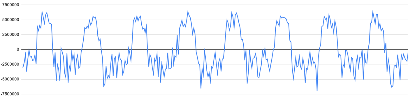
I am trying to read an analog signal using a PCM1808 and running into a very strange issue. I am feeding a sine wave (centered around 2.5v) into the chip and reading back an extremely distorted signal through the I2S interface. More confusingly, the distortion appears to be highly asymmetrical, with the "negative half" of the waveform experiencing far more distortion. Below is a screengrab of the I2S data:

As a sanity check, here is the input signal, recorded directly at the chip. 2.5vpp 1khz.

My design is essentially just the reference design, and I have verified that power / ground supplies are stable.

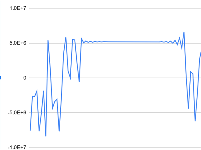
I have also noticed that at points, the input appears to "freeze" and experiences ringing. The strange thing is that this ringing seems to happen at the beginning and end of the frozen section, as if it's able to anticipate the "un-freezing", which leads me to think that something is happening internally in the chip? Below is a graph of the i2s data when being fed a slower 100hz sine wave. As you can see, it appears to freeze for ~100 samples, and rings at the beginning and end:

I really have no idea what's going on- I would almost be inclined to assume that I have a damaged part / board, except for the fact that I have two of them and they're behaving identically. If anyone has seen something like this before or can suggest anything to try, please let me know!

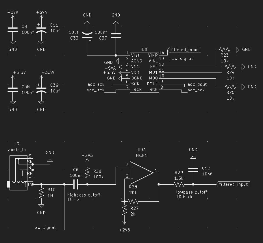
EDIT: Here is the relevant portion of my schematic, including input amplification. As you can see, it is nearly identical to the reference implementation. I am seeing identical behavior on both inputs (raw and 11x amplification), though the above screenshots have been from the amplified source. I've also tried adding a 0.1uf cap between the signal and chip input pin to see if that makes a difference, but that didn't solve the issue.

Thanks!

  • Hi Conrad,

    Can you share your schematic? 

  • Hi Daveon, I've added the schematic to my post. Thank you for taking a look!

  • Hi Conrad,

    Your schematic looks good, nothing stands out that would warrant the distortion in the output.

    What are you I2S clock frequencies? Your providing an SCKI while the device is in slave mode, is this intentional?

    Regards

  • Hi Daveon, I've been using 32ks/s (LRCK=32KHz, BCK=2.048 MHz, SCK=8.192MHz) but have tried a few other sample rates and seen similar behavior. I was under the impression that the SCK needed to be provided in slave mode, but if it's not needed, that's an easy test to run tomorrow!

  • Hi Conrad,

    My mistake SCKI is required for this device in slave mode.

    Also the BCLK may be incorrect, at 32kHz Fs * 24bit word length * 2Ch, BCLK should be 1.536MHz

    I suggest changing the frequency and testing that the clock signals are a stable 1.536MHz BCLK, 8.192MHz SCK, and 32kHz Fs because your output is matching the expected response of unsynchronized frequencies.

    Example below:

    Regards,

  • Hi Daveon,

    Sorry for the delayed reply. I've been using the 32-bit word length (or 64 bck/frame as the datasheet puts it), which I believe is supported:

    I've been driving the clock signals from an MCU, so base-2-divisible clocks seemed like the easier option. I tried using the 24bit format on Friday but found that the chip would display similar behavior as to before. I'll try again later today with some different clock frequencies to see if I can get anything to work.

  • I do see something in the schematic that may be causing your troubles.  VINL is directly connected to your audio input.  If the source is capable of driving the input below -0.3V then this can cause strange behavior on the adjacent channel.

    If you use a capacitor in series with VINL this will allow proper operation, as the inputs are internally biased to Vcc/2, or you can leave it disconnected if not used.  Alternatively you can tie VINL and VINR together, and get a 3dB boost in dynamic range by numerically summing the output data.

    VREF is a low-noise reference at Vcc/2, you can use this for your +2V5 reference but it will have to be buffered first with a unity-gain op-amp.

    The "freezing" phenomenon is numeric saturation in the decimator, e.g. clipping.  The ringing artifacts seen at the beginning and end of the clipping is a result of the linear-phase digital filters limiting the frequency response in the output data.  This is normal behavior.

    The original clock frequencies you mentioned are good, as long as they are stable and synchronous with each other.

  • Hi Jeff,

    Thank you for taking a look at my schematic! This sounds very promising, and I would suspect that it's the source of the problems that I'm seeing. I'd initially connected up the raw signal as a fallback for debugging, so it's amusing that this could be what's causing all of my issues.

    Due to my PCB design, testing this will likely require some "advanced rework", so I will update in a few days when I can test it.

    Thanks again

    Conrad

    EDIT:

    After testing, this indeed solved the issue. Thank you!

  • Conrad,

    That's fantastic.  Glad to hear it worked out!