This thread has been locked.

If you have a related question, please click the "Ask a related question" button in the top right corner. The newly created question will be automatically linked to this question.

TAC5112: routing and gain setting questions

Part Number: TAC5112

Tool/software:

Hello,

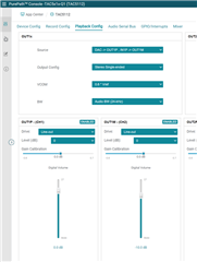
My customer would like to have two audio paths, IN1P/M to OUT1P/M loopback and I2C to OUT1P/M, simultaneously as below. The IN1P/M to OUT1P/M loopback gain is -10dB and the I2C to OUT1P/M gain is 0dB respectively. Is this doable? If yes, could you provide a PPC3 configuration file to meet their requirements, please?
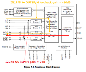

Best regards,

K.Hirano

  • Hi Hirano,

    There is a provision made in PPC3 for this exact routing. Screenshot below:

    The gain will be applied in the DAC signal chain through digital volume control, shown in the screenshot as -10dB gain is applied to signal sourced from IN1M.

    I will update this thread with a script that entails all the registers needed for this configuration to operate correctly asap.

    Thanks,

  • Daveon,

    Thank you very much for taking care of this.
    I look forward to receiving the script.

    Best regards,

    K.Hirano

  • Hi Hirano,

    To update, please try the script attached. 

    ##############################
    
    w a0 00 00	# Go to Page 0
    w a0 01 01	# Software Reset
    w a0 02 09	# Wake up with AVDD >2V & all VDDIO levels
    w a0 10 E0	# Loopback Enabled
    w a0 19 00	# 1 data input, 1 data output for PASI
    w a0 1a 30	# PASI TDM , 32bit format
    w a0 1e 20	# PASI CH1 on slot 0
    
    ### Mixer Configuration #####
    
    w a0 00 0a		# Go to page 10
    w a0 08 7F FF FF FF	# Enable ADC CH1 Mixer
    w a0 48 7F FF FF FF	# Enable ADC-DAC loopback for ADC Ch1 
    w a0 00 11 		# Go to page 17
    w a0 58 00 00 40 00	# Route ADC LOOPBACK CH1 to LDAC
    w a0 08 40 00 00 00	# Route TDM CH1 to RDAC
    w a0 10 00 00 00 00 	# cutting off TDM CH2 to RDAC
    
    #############################
    
    w a0 00 01	# Go to Page 1
    w a0 2c 70	# Sidechain, loopback, Ch mixer en
    w a0 00 00 	# Go to page 0
    w a0 64 24	# Input from DAC and Analog signal path, Stereo SE, changed
    w a0 65 e0	# FD/RECEIV drive, LDAC - OUT1P (ADC input)
    w a0 66 e0	# FD/RECEIV drive, RDAC - OUT1M (TDM CH1)
    w a0 67 b5	# DVOL OUT1P-> ADC input, -10 dB DVOL
    w a0 69 c9	# DVOL OUT1M-> TDM input CH1, 0 dB DVOL
    
    w a0 76 8c	# ADC CH1 and DAC CH1-LDAC, CH2-RDAC is turned on
    w a0 78 c0	# Turn on ADC/DAC

    This device is currently in a preview stage, when fully available to the public an application note detailing how to configure the loopback function and routing options will be available in the product folder.

  • Daveon,

    Thank you for providing the script
    However, first of all, they would also like to confirm what kind of path can be achieved or not.

    Could you show this loopback path in a block diagram such as section 7.3.7.1 ADC Signal-Chain (Figure 7-17) and section 7.3.7.2 DAC Signal-Chain (Figure 7-32) of the TAC5112 data sheet, please?

    Best regards,

    K.Hirano

  • Hi Hirano,

    The loopback path is present in the image.

  • Daveon,

    Thank you for your response.
    My customer thinks the block diagram as attached pdf. Is their understanding correct?
    CODEC_SideTone.pdf
    And they would also like to confirm if the IN1P/M to OUT1P/M loopback path volume can be adjusted independently of the I2C to OUT1P/M path volume, before the adder.

    Best regards,

    K.Hirano

  • Hi Hirano,

    The loopback from the ADC actually occurs after the biquads in the ADC signal chain and the data is inserted following the biquads in the DAC signal chain. I have made a note to revise this in the datasheet. The block following the adder is where the DVOL control takes place.

    Yes the DVOL can be adjusted for outputs independently, an example is shown in the first screenshot.

    Regards,

  • Daveon,

    I am confused.
    If the following the adder is where the DVOL is, then the DVOL affects both signals simultaneously. To control the gain independently, one DVOL must be located for ADC path before the adder and the other DVOL has to be located before the adder for DAC path as described in the CODEC_SideTone.pdf.
    Please let me know if the CODEC_SideTone.pdf. is correct or not. If it is not correct, please show me a correct signal flow block diagram.

    Best regards,

    K.Hirano

  • Hirano-san,

    I've reached out to continue thread offline.

    Regards,