This thread has been locked.

If you have a related question, please click the "Ask a related question" button in the top right corner. The newly created question will be automatically linked to this question.

TLV320ADC6140: What's the max capacitance loading for BCLK

Part Number: TLV320ADC6140

Tool/software:

Hi, Team

Our customer use TLV320ADC6140 in their project, and they meet some EMI issues.

after check, they found the issue maybe caused by the BCLK (BCLK fw is 24.576M Hz). the BCLK waveform shows that the BCLK signal waveform is distorted, and they believe it is caused by signal reflection. If the PCB is not good enough, it has the signal reflection. But as the PCB is fixed, they prefer add a cap to the BCLK to improve the signal quality.

Pls check their test as below:

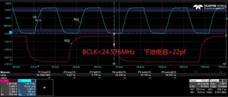
Test 1: add 22pF to the BCLK pin.

Test 2: add 47PF to the BCLK pin.

From the 22pF and 47pF cap test, we can see that the 22pF cap is better even though it has some distorted.

My customer prefer check with us for below question:

1, For 22pF can 47pF cap waveform, Do you think this waveform will affect the normal operation of ADC6140 ? pls note the waveform has some distortion, but the rise/falling time can match our datasheet.

2, What's the max capacitance loading for BCLK? ADC6140 datasheet shows (in "7.10 Timing Requirements: TDM, I2S or LJ Interface") ADC6140 I2S timing test  is base on condition for cap loading is 20pF. Customer prefer to check whether 20pF is the max cap loading for BCLK? 

3, do u have any others ideas to improve the BCLK performance besides optimizing the PCB?

Thanks.

G.W

  • Hi G.W,

    When the device is in TDM/I2S master mode the digital output capacitive load is 20pF - 50pF. When the device is in slave mode digital input pin capacitive load is 5pF. However, as shown in the typical application circuit, we don't recommend capacitors on the audio serial bus. Larger capacitors on SDOUT and incoming clock signal traces can induce distortion in the audio data. 

    , For 22pF can 47pF cap waveform, Do you think this waveform will affect the normal operation of ADC6140 ? pls note the waveform has some distortion, but the rise/falling time can match our datashee

    Yes, as shown in your diagram, the capacitive load is softening the edges of your clock signals. SDOUT data is latched onto the edges on BCLK so as the signal distorts, so does the output audio signal.

    2. The max capacitive load is dependent on whether the device is configured for slave or master mode. 

    3. There are many factors that contribute to EMI susceptibility and PCB layout is a large factor. But, minimizing high frequency switching signals is paramount as well. I2S clock signals when clean and stable into an audio ADC should not generate massive EMI complications. Does the ADC feed into a digital input speaker amp as well?

    Also, is the BCLK snippet provided a capture of the output in master mode? If so, please attach your schematic.

    Regards,