Tool/software:
Hello,dear expert:
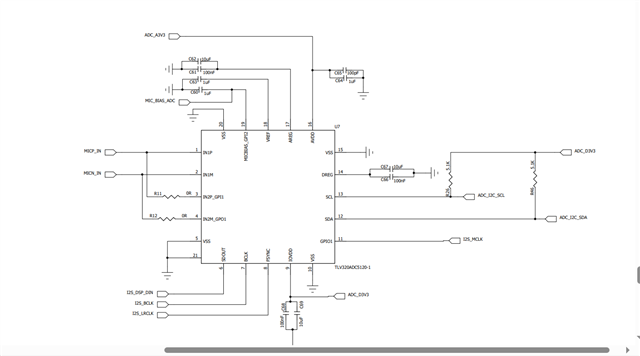
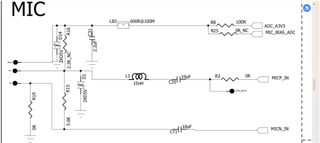
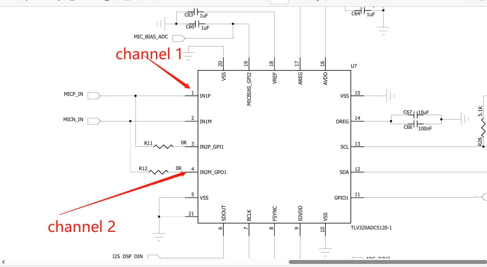
Our microphone project, one transmition and one receiver. The transmition use 5120, 5120 I2S output to telink. The receiver is telink UAC output.
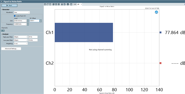
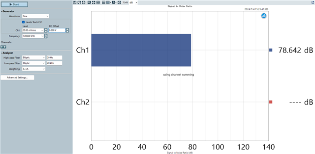
Now we encounter problem.It's when input small signal such 5mvrms, THD+N is below 0.2%.But we see frequency spectrum on ap, the interference
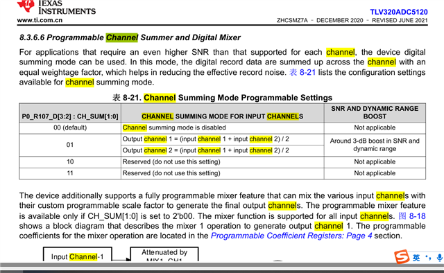
is big,as following picture.According to 5120 datasheet, enable dre will help optimize this problem, write 0x25 data to 0x3c register,write 0x81 data to 0x6d register.
The actual test result is that when input small signal such 500uvrms,the gain is no change.The attachment is 5120 init code.Please help to check and help
resolve the problem.Thank you!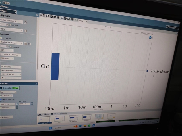
void TLV320ADC_Init(void)
{
    //w 9c 00 00 # Goto Page 0
    //w 9c 02 81 # Wake-up device by I2C write into P0_R2 using internal AREG
    //w 9c 6B 05 # Linear Phase Filter with 2 channel summer mode (DSP_CFG0)
    //w 9c 07 30 # TDM Mode with 32 Bits/Channel
    //w 9c 73 c0 # Enable Ch.1 - Ch.2
    //w 9c 74 c0 # Enable Ch.1 - Ch.2 ASI Output channels
    //w 9c 75 e0 # Power up ADC
    u8 r_data;
    u8 wack;

    TLV320ADC_i2c_init();

    wack = TLV320ADC_IIC_WriteReg(0x00,0x00);
    if(wack == 0)
        my_dump_str_data(1,"============set page0 fail", 0, 0);
    if(wack == 1)
        my_dump_str_data(1,"============set page0 succ", 0, 0);

    TLV320ADC_IIC_WriteReg(0x02,0x81); // Wake-up device
    TLV320ADC_IIC_WriteReg(0x6b,0x01); //


    //ADC_IIC_WriteReg(0x07,0x30); // TDM Mode with 32 Bits/Channel
    //TLV320ADC_IIC_WriteReg(0x07,0x40); // IIS Mode with 16 Bits/Channel
    TLV320ADC_IIC_WriteReg(0x07,0x60); // IIS Mode with 24 Bits/Channel
    TLV320ADC_IIC_WriteReg(0x13,0x01); // MCLK = 12.288 MHz, slave mode, auto clock configuration is enabled, automatic mode pll, fs is 48KHz
    TLV320ADC_IIC_WriteReg(0x14,0x44); // BCLK = 3.072 MHz , 48KHz
    // channel 1 config
    //TLV320ADC_IIC_WriteReg(0x3c,0x24); // Analog single-ended input, AC-coupled input  10-k   input impedance
   //TLV320ADC_IIC_WriteReg(0x3c,0x04);   // Analog differential input  10-k   input impedance, analog differential input, dre/agc/drc disabled

    // DRE or AGC or DRC enabled based on the configuration of bit 3 in register 108(P0_R108)
   TLV320ADC_IIC_WriteReg(0x3c,0x25); // Analog single-ended input, AC-coupled input  10-k   input impedance
   TLV320ADC_IIC_WriteReg(0x6d,0x81); // Input signal level threshold is -60 db, Maximum gain is 4 db


     // TLV320ADC_IIC_WriteReg(0x3d,(0<<1));// Channel gain is set to 0 dB
    //TLV320ADC_IIC_WriteReg(0x3d,(12<<1));// Channel gain is set to 6 dB
    //TLV320ADC_IIC_WriteReg(0x3d,(6<<1));// Channel gain is set to 3 dB
    TLV320ADC_IIC_WriteReg(0x3d,(0<<1));// Channel gain is set to 0 dB


    TLV320ADC_IIC_WriteReg(0x3e,0xc9); // Digital volume control is set to 0 dB
    //TLV320ADC_IIC_WriteReg(0x3e,205);   // Digital volume control is set to 2 dB
    //TLV320ADC_IIC_WriteReg(0x3e,0xff);   // Digital volume control is set to 27 dB
    //TLV320ADC_IIC_WriteReg(0x3f,0x80); // Gain calibration is set to 0 dB
    //TLV320ADC_IIC_WriteReg(0x40,0x00); // No phase calibration

    TLV320ADC_IIC_WriteReg(0x73,0x80); // Enable Ch.1
    TLV320ADC_IIC_WriteReg(0x74,0x80); // Channel 1 output slot is enabled
    TLV320ADC_IIC_WriteReg(0x75,0xe0); // Power up ADC, PLL, MICBIAS
}