Part Number: LM4950
Tool/software:
hi Expert,
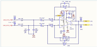
We have the schematic design as the following, please help me check if it is ok, any potential issue?
Best rgds,
KPK
This thread has been locked.
If you have a related question, please click the "Ask a related question" button in the top right corner. The newly created question will be automatically linked to this question.
Part Number: LM4950
Tool/software:
hi Expert,
We have the schematic design as the following, please help me check if it is ok, any potential issue?

Best rgds,
KPK
Hi KPK,
1. C71 is 470uF, this large of a value cap is not needed. Feel free to use a smaller one to lower cost and space.
2. We recommend replacing R97 and R101 with 20k resistors. Then you ca adjust the feedback resistor to account for your desired gain. Thanks.
Just a note: Data sheet mentions minimum of 4Ohm for single-ended output and 8Ohm for differential output.
Regards,
Sam
Hi Gu,
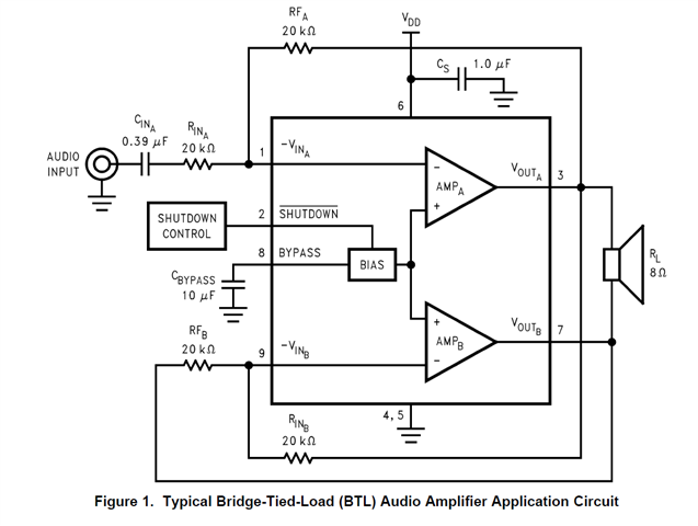
Yes, you can use differential input. Please note that in the Figure 1 circuit, the input into AmpB is the inverted signal of AmpA. In your case, you need to make sure your input signals are 180 degrees out of phase with each other. Also, you can see RFB and RinB are the same value, 20k, this is too provide unity gain. The sole purpose of this amplifier is to drive the output differentially. The filter's cutoff frequency is fc = 1/(2πRINCIN). You can check out page 16 of the datasheet for more information.
In your schematic you should adjust the values of R92 and R97 to configure the closed loop gain of AMPA, and you should replace R101 and R105 with two 20k resistors to the gain of the second amplifier to be -1. After determining the gain of AMPA you should refer to the SELECTING EXTERNAL COMPONENTS section for an explanation on how to determine the value of the input coupling capacitors and bypass capacitors.
Your C71, the supply bypass capacitor is very large. Please try to replace the 470uF with a 10uF.
Thanks.
Regards,
Sam
Hi, Sam,
You may misunderstand my schamatic.
Pleae note on my schematic DNE (means do not emplement), so R105 is not mounted.
R92/R97 is gain for AmpA, R104/R101 is gain for AmpB,
R92=R104=51K, R97=R101=10K
My input for AmpA is Line_OutL_P, and AmpB is Line_OutL_N, they are in opposite phase.
Please advise if it is ok, as it different with typical application circuit in datasheet.
Thanks and best regards
Gu HaiLin
Hi hailin,
Thank you for your clarification. Is it good that your inputs are opposite phase. However, AmpB's gain needs to be configured to be -1. In your schematic AmpB has a gain that is not unity gain. AmpA's output serves as AmpB's input, so the result is that both amplifiers produce signals identical in magnitude, but 180 degrees out of phase. Thanks.
Regards,
Sam
Hi Gu
I have reviewed your schematic. It varies drastically from the typical application we recommend. We do not recommend that you use this device in this configuration. AmpB needs to have a unity gain of -1 to drive the output differentially. Thanks.
Regards,
Sam