This thread has been locked.
If you have a related question, please click the "Ask a related question" button in the top right corner. The newly created question will be automatically linked to this question.
Tool/software:
Dear Expert
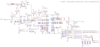
When our project team is using TI's audio transceiver DIX4192 chip, we use STM32's SPI communication. After configuring to 8-bit and 16 bit, we cannot successfully issue commands to set registers.
For example, I want to set DIX4192 as the master and use MCLK as the master clock to output to port A and port B, but after configuring the ports, AB does not have clock output.
Even if configured to output audio from port A to AESOUT in DIT, there is no clock on SYNC and RLCK.
I would like to ask about SPI configuration (CPM down) and CS chip selection, as well as RESET setting, register configuration, sending three bytes each time, lowering chip selection before sending, and raising chip selection after sending. What other configurations are needed?
Could you please send us the detailed configuration process? Can DIX4192 configure I2S audio to A input and B output to achieve its own MIC input and SPK output?
Also attached, our sending data
w 7F 00 00
w 03 00 09
w 05 00 29
w 09 00 01
w 0D 00 0B
w 0F 00 12
w 10 00 00
w 11 00 00
w 1B 00 0A
w 1C 00 00
w 1D 00 01
w 01 00 3E
w 0E 00 01
Hi Gabriel,
I went through the code that you have provided and i did not see any issue except i am not sure if your input is at RX4 .I added the descriptions to each register for easy reference and quick check.
You can set the part by setting CPM to 0 for SPI mode, Reset (active low) set to High and Chip select (active low) to LOW for SPI mode ( you can toggle them to these final values before sending data)
Can you also provide RXCLK along with MCLK and check the result (refer to Figure 69. Typical Application Diagram Using SPI Host Interface)
If still not working, refering to Figure 11. Digital Interface Transmitter (DIT) Functional Block Diagram, try to mux the RX4 to TX or AESOUT and see if you get any output at any of those pins ( just a sanity check)
I found this simple script for this device that might be useful to test your set up with.
Here is the detail of your code with some caption:
w 7F 00 page 0
w 03 09 I2S ,master, PART A is source, not muted
w 05 29 I2S ,master, DIR is source (NOT THE DEFAULT) , not muted
w 09 01 The buffers are updated through the SPI or I 2C host interface
w 0D 0B Rx Ref Clock: MCKI , input : RX4
w 0F 12 these 3 registers give these values for P=1 J=8 D=0
w 10 00
w 11 00
Registers 0x0F through 0x11 are used to program PLL1 in the DIR core. PLL1 multiplies the DIR reference clock source to an oversampling rate which is adequate for AES3 decoder operation.
PLL1 is programmed using the following relationship: (CLOCK × K) / P = 98.304 MHz
where: CLOCK = frequency of the DIR reference clock source. K = J.D
from above K=8.0 so CLOCK= 98.304 MHz /8=12.288 MHz which matches with Table 19. for clock rate and k and P coefficients.
Since D=0 , it also satisfy the condition of 2 MHz ≤ (CLOCK / P) ≤ 20 MHz and 4 ≤ J ≤ 55
w 1B 0A Receiver block start clock (GPO1 is forced low (default))
w 1C 00 GPO2 is forced low (default)
w 1D 01 GPO3 is forced high (GPO3 is forced low (default))
w 01 3E Reset 0: Disabled, PDALLZ =1 (All Function Power-Down Mode disabled so all function blocks will operate normally) PDPAZ=1 (Port A Power-Down Mode disabled so all function blocks will operate normally) PDPBZ=1 (Port B Power-Down Mode disabled so all function blocks will operate normally) Rx & Tx Power-Down Mode disabled,
w 0E 01 The recovered master clock is available at RXCKO
Dear Arash
The I2C mode has also been debugged for a long time now. The I2C sending address 0xE0, register address 0x7F, and data 0x00 did not receive an ACK (as shown in the following figure).
I2C is a simulated I2C using the original SPI pins, waiting for ACK timeout set to 250US, but no ACK has been received.
Last time, SPI also configured registers according to the example, but there was no clock output. Please share my situation again on the forum, hoping that experts can provide good suggestions. If you need a schematic, you can also send it out.
Hello Gabriel,
Could you please ask your customer to comment on my specific questions that I asked above when they are using SPI ? We need to have few things cleared so we can find the root cause. If they did and still it is not working, that is fine but i need to know so we can eliminate some of the possibilities. I repeat them here
Can you also provide RXCLK along with MCLK and check the result (refer to Figure 69. Typical Application Diagram Using SPI Host Interface)
If still not working, refering to Figure 11. Digital Interface Transmitter (DIT) Functional Block Diagram, try to mux the RX4 to TX or AESOUT and see if you get any output at any of those pins ( just a sanity check)
I found this simple script for this device that might be useful to test your set up with.
Also if I understand correctly, they are not getting ACK on the very first line of the code I sent. In the past I had experience with a different part that a lack of clk (like MCLK) was causing I2C sending NACK and it was very surprising to me!
Regards,
Arash
Dear Arash
Hello, thank you very much for your and the expert's prompt response.
We provide MCLK to DIX4192, but we do not use RXCKI. We use RXCKO and LRCKA instead, BCKA,LCKB、BCKB, I hope DIX4192 can provide the clock.
However, after configuring through SPI, these clocks did not output. Here is our schematic diagram.
And SPI has been tested using a simple script according to expert opinions, but it still does not work. Finally, I2C communication did not receive an ACK, and MCLK works normally, with output provided by the crystal oscillator.
Can the experts help take a look at our schematic diagram.
Hello Gabriel.
I looked at the schematics and I am not clear exactly what is trying to be achieved, Isn't PORTA in MASTER mode per script?
According to reg 03 it is set in MS mode. In Master mode, the LRCK and BCK clocks are outputs, derived from the Port A master clock source.
Please read section 9.3.2. , I kept asking to provide both MCLK and RXCKI and I don't see that is followed.
The DIX4192 includes two clock inputs, MCLK (pin 25) and RXCKI (pin 13). The MCLK clock input is typically
used as the master clock source for the audio serial ports and/or the DIT. The MCLK may also be used as the
reference clock for the DIR. The RXCKI clock input is typically used for the DIR reference clock source, although
it may also be used as the master or reference clock source for the audio serial ports.
My final recommendation to them is that you need to provide RXCKI as I have asked in my previous posts.
Regards,
Arash