This thread has been locked.

If you have a related question, please click the "Ask a related question" button in the top right corner. The newly created question will be automatically linked to this question.

PCM1754: The output stepped after muted

Part Number: PCM1754

Tool/software:

Hi experts,

I met a problem with PCM1754, its output voltage stepped after has been muted for 9ms. This kind of step change of output voltage will result problem with following power amplifier. It has been confirmed the I2S communication has been stopped before and after mute signal. What is the reason of this output voltage step? below is the waveform scoped at VOUT pin.
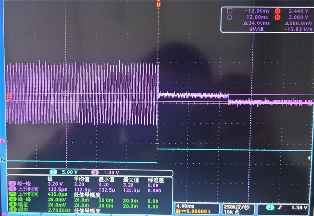
In the picture, channel 2 (blue) is MUTE, channel 3 (red) is VOUT. In which you can find right after MUTE issued, the VOUT level is about 2.5V, this is expected. However, the problem is about 9ms after MUTE, the VOUT level stepped from 2.5V to 2.1V. What is the reason of this stepping? how to avoid it?

Thank you,

John

  • Hi John,

    Can you monitor the VCOM pin and make sure there is no issue with its decoupling and it is stable. Also monitor the supply pin  since you have confirmed all clks are stopped at the point of occurrence.

    Is this 9ms repeatable? That is, do  you always get the step  after 9ms or this number changes after each reset or power down/up?

    Regards,

    Arash

  • Hi Arash,

    Thank you for reply. Yes VCOM is always stably 2.5V either in normal operation and after muted. VCOM pin has been decoupled to GND through a 10uF cap. Supply voltage is correct. The reason why all clks are stopped is the interface device which drive I2S i/f is disabled. 

    Yes, 9ms problem is repeatable. 

    Regards,

    John

  • Hi Arash,

    I am sorry, some information I previously said is not correct. I have engineer done some further test.

    The fact is the I2S signal is not shut off when MUTE is issued. The cause of step is clear. The system shut off I2S signal 9ms after MUTE, and before MUTE signal system has write PCM1754 to 2.5V out. The question is why 0.4V step occurred when shutting off I2S signal though it has been muted?

    Also I have engineer done another test: send MUTE signal when the DAC is set to other value than 2.5V, wait for 9ms delay, and then shut off I2S. The result is VOUT level after mute (and I2S is still on) is correctly 2.5V, while with I2S shutting off (in MUTE status), a 0.4V step occurred on VOUT. The step can be steadily repeat, but the step may be +0.4V or -0.4V.

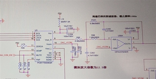
    This 0.4V step is not allowed, what should be done to avoid it? Below I attached the newly tested waveform and the schematic.

    Thank you!

    John

  • Hello John,

    I am wondering if VCOM is changing at all when you shut off I2S. 

    1)please remove the attachment to the DAC and only put a LOW pass filter with appropriate fc attached to it . Monitor the output with or without I2S

    2) For the second part with your above circuit, do not use VCOM for the input of the opamp. This will be similar to the  app note circuit below:

    app note schematics

    Let me know how the output is behaving once you mute it ( with or without I2S) 

    In all cases monitor the VCOM.

    Regards,

    Arash

  • Hi Arash,

    VCOM is stable, it is always 2.5V, no any issue with it.

    1) Which attachement to the DAC do you meant? The op amp is used for LPF and it has been checked working properly. 

    2) The two wavefrom was get from same part. The step is not same each time. Some time it step up 0.4V, some other times it step down 0.4V. The VCOM is connected to noninverting input of op amp, which is high impedance, no any load effect to VCOM. There is no problem with this kind of connection. The app note schematics you mentioned is incorrect.

    Regards,

    John


  • John, by removing attachment of the DAC , I meant remove the active filter that you have  attached to the DAC, then just add a simple passive LPF. For the second test, with the original active filter, I wanted to see if you connect the VINP of the amp to GND,  you would see  any difference, but since you  confirmed VCOM is not changing at all, this test probably  will not yield any additional data point.

    Also, to further debug the cause, do not shut down the I2S signals all together, do one at a time and see if a specific signal, including SCK is the cause.

    Regards,

    Arash

  • Hi Arash,

    Further test was done, here is the result:

    In this scoped waveform you can find, VOUTL muted to 2.5V as expected, while it stepped 0.4V down as I2S signal is shutting off. And throughout full process the VCOM output (yellow) is stably at 2.5V, no any.

    Another test was done keeping I2S working and make MUTE=H (connect to VCC directly). At this condition VOUTL is muted at 2.5V continuously. And then we try to short I2S signal one by one to GND. The result is VOUT keeps unchanged when we short SCK, BCK, and DATA input to GND. 0.4V step occurred once we short LRCK to GND. The direction of stepping is random but always 0.4V, sometimes +0.4V, some others -0.4V. The effect on VOUTR is same, but step direction always opposite, +0.4V step occurred on R channel while -0.4V step on L channel, and vice versa. Seems like there is Quantum Entanglement effect Slight smile

    Thank you!

    John

  • Hi John,

    This is really strange that lack of LRCLK moves  the outputs from the CM! if any, I was expecting , it would be the master clk that could effect the DAC clk.

    This is a very mature device and I don't recall we have ever seen this issue. May be it is a board related issue or  there is some charge injected on the output lines . 

    Have you changed the order of stopping these clks in different combinations?  That is, instead of  turning them off  one at a time ( while all other signals are on) , do it in a sequential  way, for example turn off sck first and then turn off LRCK and then turn off  the input signal, or another configuration turn off  Din, then BK and then LRCLK.

    I am not sure what is causing this,  but more experiments can provide additional data point and then we have a better chance to find the culprit  or a possible  work around .

    I am still  wondering if you remove the active filter, does it effect the problem?

    Regards,

    Arash

  • Hi Arash,

    Yes, we had tried many times with different order to stop I2S signal. Obviously, it is unrelated to the order.

    The active filter is not removed. I checked its operation, it works properly as expected. It does not make any sense to remove it.

    And obviously the issue is not due to any kind of charge injection. Charge injection can result some kind of transient phenomenon. While the issue is a DC effect. And there is not any reason to due the issue to board. 

    I think so far all the external factors can be ruled out. This device typically is used in audio application, in which I2S is always continuous, or audio application do not care such kind of step this is the reason why no other customer reported this issue before. My customer's application is special, it is not audio application. They care such kind of step. Could you please help me find out the reason of this step in point view of DAC itself? and based on the reason maybe we can find some work around. Or, even if there is no solution for this issue, it is also acceptable if we understand the reason. Our debug cannot stopped at some assumption.

    Thank you!

    John

  • Hi John,

    This device is very old, we do not have any information about the internal design and schematics, so there is no way we can take a look at the schematics to  figure out the behavior .  In our debug process we always isolate the DAC and occasionally we have found the circuit attached to the DAC  caused the  issue, whether it was a simple active filter, a bad capacitor , or ...   . When device is not being driven, there is  possibility of voltage coupling( not injection as I typed) to the outputs on the board  ,  but if you believe the layout is good enough, then it is good..

    Going back to the chip itself, this is an audio DAC and if  the I2S is disconnected, internally it might go into an unknown state that it needs to be reset again by providing the I2S or rest  and in the meanwhile the output might behave strangely until it is reset. Probably that is what  happening now.  Since you have confirmed the chip needs  LRCLK,  my only recommendation is to provide it to the chip. 

    Regards,

    Arash

  • Hi Arash,

    Thank you anyway.

    Our test results shown the step in VOUT_L and VOUT_R is directly related to LRCK. Once LRCK shorted to GND, at the same time VOUT_L and VOUT_R stepped up/down (the step direction of two VOUT are always complementary), and once LRCK signal released, the two outputs may step back to 2.5V. There is not any possibility for external circuit to result such kind of issue. We can do experiment if you can figure out any possibility. 

    It seems you misunderstand my description. The I2S signal is not disconnected, it is just halted asynchronously. It is possible a wrong data is latched into DAC due to asynchronous halt of I2S or just LRCLK. However, the DAC out is muted, the wrong data should not result any change of VOUT.

    The issue can be easily replicated. Cold you please test with EVM?

    Thank you!

    John

  • John,

    Sorry for delay in response, I was out for couple of days.

    My thinking is that with DAC being muted, wrong or correct data should not matter . Once  the DAC is muted it  should pull tou outputs to VCM. Also  you repeated this test few times and it always goes into a delta of 0.4V in a complementary fashion for outp and outm , it means it is not related to the wrong input being latched.

    However, I don't know once  LRCK is halted,  whether the DAC goes into an undefined  state,  such that the vout can not be pulled to VCOM. Your test shows this is the case though.  We are planning to work on EVM for few parts in the near future  and PCM1754 is one of them. 

    Regards,

    Arash

  • Hi Arash,

    Thank you! Good to know you will working on EVM. Waiting for your results. 

    Regards,

    John

  • Thanks John. 

    Regards,

    Arash

  • Hi Arash,

    Have you tested this issue on EVM? 

    Thank you!

    John

  • Hi John,

    I think there was a misunderstanding above, I mentioned above the plan is to work on several EVMs in the near future including the EVM for this part. This probably  will happen sometimes in 2025 depending on changing priorities. I can not give you a specific date. 

    Regards,

    Arash

  • Hi Arash,

    It is a very simple test, can be finished in several minutes. Could you please help to do a test as soon as possible?

    Thank you!

    John