This thread has been locked.

If you have a related question, please click the "Ask a related question" button in the top right corner. The newly created question will be automatically linked to this question.

TPA3255: TPA3255 burned down issue

Part Number: TPA3255

Tool/software:

Hi Teams,

The customer is using TPA3255 amplifier chips for subwoofers (PBTL mode). Currently, there are about 1500 units produced, and 2pcs of amplifier chips have been burned out and the damage is basically the same. The cause is being analyzed.
May I ask if there is any information about the pressure specifications that the chip can withstand when making heat sinks and the allowable PCB board deformation.
The customer's amplifier power supply uses PVDD=52V. When playing dynamic music, the maximum voltage measured at the PVDD pin of the chip does not exceed 55V. Is it considered to exceed the normal specification value of 53.5V (the extreme specification value is 69V).
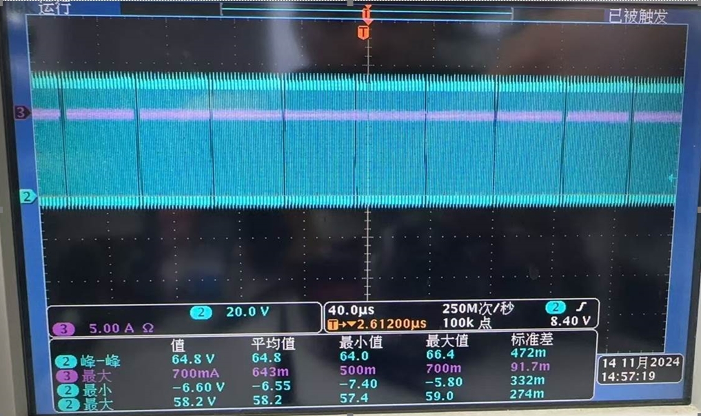
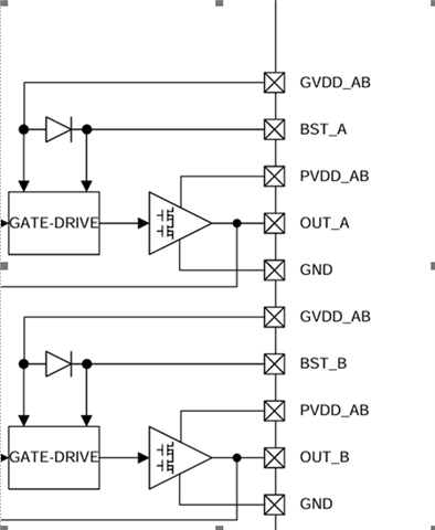
Also, using an oscilloscope to test that the low level between GVDD_AB and BST_A (the same for the other groups) is -6~-7V, is this normal and how can it be explained?

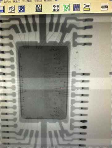
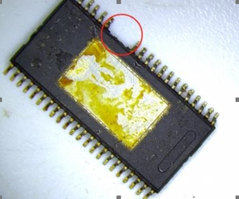
The damaged chip and X-ray photos are as follows (the yellow substance on the chip is rosin left behind when disassembling the chip)

Use an oscilloscope to test the waveform of -6~-7V at low level between GVDD_AB and BSTAA (the same for other groups):

  • Hi Vayne,

    The EVM uses a heatsink with a 1mm spacing for the IC so there are no issues if the customer is using the same height. There is not any data I have currently for maximum pressure since we expect customers to use a heatsink with the same height, but we know the device can withstand at least 100N as from this E2E.

    You mentioned that the PVDD can get to 55V. As mentioned under the abs_max section of the datasheet we cannot guarantee "functional operation of the device at any conditions beyond those indicated under Recommended operating conditions". 55V is above those limits if using a 4 Ohm load.

    The GVDD and BST voltage difference is normal. The GVDD is used to charge the bootstrap cap to a higher voltage which is then used to turn on the high side FETs. This means when the PWM is LOW the BST voltage and the GVDD voltage should be similar. When the PWM is high, the bootstrap cap is not being used for the gate drive so you see a voltage differential between the bst pin and the GVDD pin since the diode on GVDD is reverse biased.

    Regards,

    Ramsey