TPA3139D2EVM: Validating plimit

Part Number: TPA3139D2EVM
Other Parts Discussed in Thread: TLV320AIC3254

Tool/software:

Hi,

I managed to play some music on my speaker using TPA3139D2EVM. However, I needed to know how does plimit works, so I went to probe on the OUTR+ using an oscilloscope and turn the knob for plimit while having a jumper at J7, setting to IN. 

The waveform shown on the oscilloscope does not change while I changed the value at plimit from 0.4762 V to 1.5 V.

I am supplying 5V, 0.8 A on 2 speakers with 4 ohms and 2 watts each. I am seeing Vp = around 7.91 V on the oscilloscope which I think it is not the right value?  
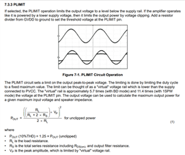


I wanted to ask how does plimit works and how can we validate the change? 

Thank you.

Regards, 
Samuel

  • Hi Samuel,

    plimit works by adjusting a "virtual rail" internal to the device. The equations in the section linked describe how to determine what the level is and how to determine what the corresponding output level will be. Are you able to send me a picture of the setup and the input/output signals? Vp can never get above the power supply so I want to make sure the signals are within reason.

    Regards,

    Ramsey

  • Hi Ramsey, 

    Here is the setting of the board:
    J7 set to enable plimit 
    J6 and J10 set to differential input mode 
    J12, J15 set to BTL
    J13 set to 20 db gain
    J14 set to low idle current

    I am using TLV320AIC3254 to send signal to TPA3139D2EVM. I have soldered the signal cables directly on C11 and C24 at RINP and LINP.

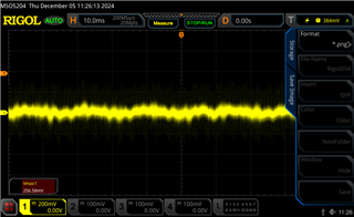
    This is the input to RINP when power supply is off.


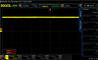
    This is the input to RINP when power supply is on, and music is playing on the speaker:


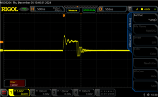
    Output:

    I am getting this for output signal when the plimit voltage is set to 0.4762V. Correct me if I'm wrong, according to the datasheet, the virtual rail should be 11.4* 0.4762 = 5.428V, but I'm only supplying 5 V and 0.8A. so I should be getting 5V for Vp ? 

    Regards,

    Samuel

  • Hi Samuel,

    It does not look like there is an audio signal going into the device. The way to validate plimit would be to play a 1kHz sine wave at full scale (max expected input level) and look at the differential output. Different plimit levels will dictate where that differential level will clip.

    If the expected rail from plimit exceeds PVDD, then the actual supply limits the output of the device. The ringing you see is likely due to an under damped LC filter, mismatched LC filter, a sensitive speaker load, or ferrite bead filters.

    Regards,

    Ramsey

  • Hi Ramsey, 

    Thanks for the explanation, from what I understand from it is adjusting plimit will change output level and plimit will determine where will voltage clipping occur.

    Currently I am facing another issue where adjusting plimit does not change the output level at OUTR+ and OUTL+. Am I supposed to see an increase in ampltiude if I increase plimit? 

    Regards,

    Samuel


  • Hi Samuel,

    You would expect to see less clipping if PLIMIT was causing clipping to begin with. If the signal level was large enough to clip on the virtual rail and the virtual rail is lower than the actual supply, then adjusting PLIMIT would increase or decrease the peak level by having more or less clipping.

    Regards,

    Ramsey