This thread has been locked.

If you have a related question, please click the "Ask a related question" button in the top right corner. The newly created question will be automatically linked to this question.

UC3846: Help with design for a 1.6KW SMPS

Part Number: UC3846


Tool/software:

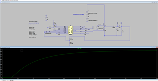
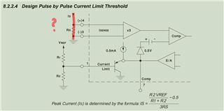
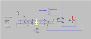
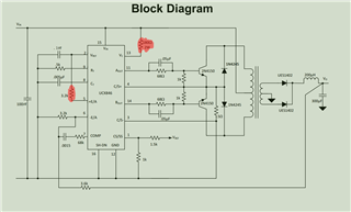
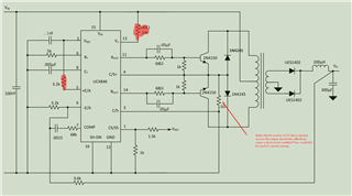
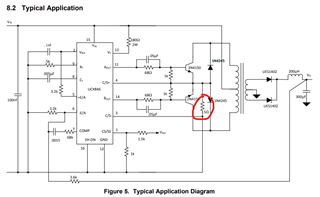
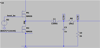
Hi there, so I've been using the UC3846 in my half bridge flyback converter design. I've been simulating it in LTSpice however I have had some trouble with the model. I'm trying to run the chip with a switching frequency of 500kHz However when probing the CT pin (which shows a ramp at the calculated frequency) I just get a dc offset? All my calculations follow the UC3846 datasheet to a tee and I have used matlab to compute them. Both are attached. I've managed to get the design somewhat working at 50KHz but the template I'm using still doesn't seem to quite work, so any recommendations on that would be highly appreciated. I also left the R and C values at the COMP pin as default as I dont know how that works yet6102.Testing.zip

  • Hi,

    Please provide your schematics for review. We are not supporting LTSpice so what we can do is to review your schematics design to see anything needs to change.


  • Hi there Hong, I've changed my schematic a bit and found a small error in my inductor formula, looks better now but still not right. I realized my High side MOSFET wasn't being activated properly because the Vgs voltage wasn't sufficient and I hadn't added a bootstrapping circuit. Here is the updated circuit with a simulated bootstrapping circuit.  

  • Hi,

    I will have review which may need a bit time. I will reply to you in about two days.

  • Thank you so much,  your efforts are greatly appreciated 

  • Hi,

    What are the values of CT and RT?

    What are the signals on CS+ and CS-?

    Can you short ILIM to GND to make debug?

    B2 is your arbitrary signal - how does this work with AOUT of UC3846?

    All in all, check each pin to make sure your circuit is correct to set up first.

  • 1. The values are on the side there in the parameters section, 5n for Ct and 8.8k for Rt. 

    2. The C/S + and C/S - current sense pins are used to measure the load current, the datasheet setup didn't make sense as it simple put it in shunt to ground.

    I have wired it in series with the output load.
     
    3. Not sure what you mean by shorting Ilim to create a debug? That would just mean making R2=0 which would make Is = (0 - 0.5)/3*Rs = -3.33A? 
    4. It is simply used as a gain to the output at Aout (Makes a PWM signal  in the high side MOSFET equal to about 330V) , since I haven't added a bootstrap circuit the high side MOSFET couldn't switch on properly due to the high input voltage of 320V at the drain of the MOSFET with a 20V PWM driving signal.
    5. I have but I don't really have a good grasp of a few things and the datasheet doesn't do anything to explain them. Example: What is the purpose of the 180 ohm resistor here and the 3.2K resistor?


  • Hi,

    Come back to your frequency question:

    Based on this below formula and Rt= 8.8k, and Ct = 0.005uF, fT(kHz) = 50 kHz, so match to your result.

    Do you have other issues needed to help to resolve?

  • Yes that is because that is the only frequency which works, its doesnt work at other frequencies. If i can get this frequency to work I'll fix that issue afterwards

  • Hi,

    I am not understanding your comment. Your Rt and Ct result is the same as the datasheet formula. So there is no issue.

  • Yes but I want a frequency of 500kHz and when I update the RT and CT to reflect that the simulation model no longer works 

  • Hi,

    As we do not support LTSpice, you would have to find out by yourself what possibly model change is needed.

    If you have a physical device with such issue, then you need to make return process. 

  • Ok I might just use a different IC because if I can't simulate it, I wont build it. In that case can you tell me the proper configuration of the current sense resistor, Rs, because the configuration in the image makes no sense. Is the datasheet wrong because I haven't seen a current sense technique with a very low value resistor in parallel to the load before?


    Then what is the purpose of these 2 resistors highlighted here? The datasheet makes no mention of the resistors besides the example and gives no hint in how to determine their values


    If you can answer those 3 questions I will be happy to call this closed, once again greatly appreciate the help

  • Hi,

    1.

    This below is just to provide a current sense idea and no indication to parallel Rs with load.

    A circuit closer to the practical is in datasheet section 8.2. You can refer to this for your design.

    I notice you have a question on this 0.5-ohm Rs. I think you need to draw a loop how current is flowing when one of bipolar transistors turn on to help you clarify there is no short circuit as you imagined. The circuit is a push-pull and no problem, you need to draw each current flow loop when one of bipolar to conduct to find out. You cannot just imagine there is a short to load - you need to show where is short if you can or there is no short.

    2 and 3.

    The 180-ohm connected to Vc has two function, (a) to limit the current to AOUT and BOUT to its max pecs and (b) to provide driving current to AOUT and BOUT. You can look at section 7.2 to understand this. Vc is a pin to provide required voltage and current to drive AOUT and BOUT.

    The 3.2k to EA+ is to balance 3.2k to EA-. This is typically a requirement in an error amplifier setup to minimize offset between EA+ and EA-. 

  • Oh I think I see, ok so just some final questions:
    1. So for the 180 olm resistor I can probably just keep it that way? If i need more current for what ever reason I can just reduce it?
    2. The 3.2k resistor we just spoke about, is there any situation which I would need to change that?
    3. Do you have any recommended material for the compensation network calculations for the COMP port? I did 2 control systems course while I was at university but it has proven difficult more me to apply it here. 
    4. Thank you so much for pointing out the current sensing issue, very stupid error on my behalf. With that taken into consideration would this be suitable setup for the Isense resistor?

    Side note: I managed to get the oscillator working properly! As it turns out even though the calculation for oscillation frequency implies I can chose any value for Rt and Ct, for the model at least anything below Rt = 4K didn't work however if I fixed Rt above 4k and changed Ct I could get it to work. Will test this in reality when I'm eventually happy with my design.


  • Hi,

    1.

    You can change 180-ohm to other values but cannot change it so low to violate current max allowed.

    2.

    3.2k is better to keep although you can change both 3.2k to a different value. I do not see a reason you need to change it.

    3.

    https://www.ti.com/lit/pdf/slva662?keyMatch=type%20ii%20and%20iii%20compensation&tisearch=universal_search

    4.

    You need to check CS+ and CS- specs not to violate their abs max.

  • Awesome, thanks so much for your help, really appreciate your time and efforts