This thread has been locked.

If you have a related question, please click the "Ask a related question" button in the top right corner. The newly created question will be automatically linked to this question.

DRV595: All signal applied but no output PWM

Part Number: DRV595

Tool/software:

Hi.

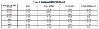
We have been using the DRV595 in several projects over the last years. Now we have a new project and encounter the same behaviour as described in the linked post. All input signals are applied, input voltage is ok, IN+/IN- as usual, Gain is ok, SDZ slew rate checked, no FAULT signal,GVDD is 7V, BUT: no output signal. Both output pins are about 900mV and no PWM or output voltage visible.

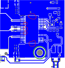
Do you have any ideas? Screenshot of schematic attached.

Best regards,

Christoph

  • Hey Christoph, 

    What is the voltage difference between the two IN- and IN+ ?

    Also, please provide a .pdf version of the schematic for a clearer image. 

    Regards,

    Ore.

  • Hey Ore, thanks for having a look at my topic.

    In all of our desgins, IN- is 0,4Vref and IN+ is changing between 0V and 0.8V for heating and cooling the TEC.

    I will send the pdf to you via PM. Hope that is ok.

    Best regards,

    Christoph

  • Hey Chris, 

    Looking at the schematic, I see the IN- cfg is loaded for transient noise decoupling which is okay, but voltage dividing a 2Vdc source into that pin seems like a problem. The DS recommends this pin should have a 3Vdc source going into the IN- pin. Right now, it seems the voltage going into this pin is outside the DS recommended operating mode. Also I strongly advice following the startup sequence in your application. I have attached images below for guide.

    It is not clear what you have on the FS pin cfg, the max recommended voltage is 0.8V and there is a scheme for desired oscillation frequencies. I have attached images below. 

    It is not clear what the operating PVCC voltage but if it is higher than the recommended FS pin voltage required, the device is not operating within the recommended conditions.

    To have a functional DRV595, I would start from fixing the bugs I have mentioned above.

    -------------------------------------------------------------------------------------------------------------------------------------------------------

    images:

    DS recommendation for IN- single-ended application:

    DS start-up sequence:

    fs pin recommendation:

    Regards,

    Ore.

  • Hey Ore, thanks for reviewing the schematic. Just to mention it again: We have been using this design in hunderts of products before without a problem. We always use the 0,4V Ref on IN- and 0...0,8V on IN+. Our power supply voltage is 24V. We always have the 100k series resistor on FS pins. I measured it the first time now and it results on 18V on the pins. I installed a pull down resistor to make the pin level 0.5V but it does not help. By the way, I copied this design from your evaluation board, and there are no pull down resistors either. So that is obviously not the problem. The only thing I could imagine is the timing from PVCC and IN+/IN-. Meeting that requirement is very hard to achive in a design. We encountered some problems in the past with the starting of the device, sometimes it catches the wrong gain config from the resistor devider. You can only resolve that problem by powering down the device and starting it again. So we installed a mosfet relais in the PVCC line to switch the device completely off and on again, but the IN+/IN- stays powered all the time.

    we will make some further tests with the IN+/IN- input timing and levels now.... keep you updated.

    best regards

    Christoph

  • Hi again. We investigated all day but could not make the DRV595 running. The biasing of the IN+ and IN- to 3V did not help. We made a lot of other tests, double-checked all components and the pinout without any luck. Still no signal on the output. GVDD is stable 7V, sync pin outputs 100kHZ signal, so internal circuits are powered and running, but the device behaves as if the outputs where HI-Z..... we will keep on searching next weeks. If you have any furter ideas, please let us know.

    best regards and have a nice weekend

    Christoph

  • Okay Christopher. I would look through the extra info provided and while you investigate, please provide .pdf format. It is hard to zoom in on the image.

    I would like to add, if the IC is not responding to the correct configuration after operating in a different/non-ideal way outside the recommended conditions, it may be hard to get the IC working again. The IC should always operate with recommended conditions. I strongly advise following the start-up sequence, if some conditions aren't met, the IC could experience some reverse bias current flows that it is not expecting. 

    I would wait till next week for an update, but please provide a .pdf file. 

    Regards,
    Ore. 

  • Good Morning Ore, I sent the schematic pdf to you via PM last week. Please check your PM inbox. Will go on testing now....

  • Hey Christoph, 

    More comments on the schematic. All this is to help ensure the IC is performing at acceptable configurations and is powered up to be functional within the specs of the DS. If IC works under conditions not met, IC may behave unpredictably:

    • Although 0.4Vdc has worked, follow the 3Vdc on IN- the DS explicitly recommends for single-ended inputs on DRV595. I also recommend matching the input impedance externally. The differential input impedance based on R1 and R2 is 30K. I would recommend using a simple impedance matching cfg for better voltage sensing at the input. For example, 15kOhms to gnd on each input terminal near the IC input. This is common practice for amplifiers.
    • I also recommend decoupling GVDD before reaching the resistor divider circuit. GVDD is a power output pin and should be treated like a power source from the IC.
    • Connect an rc circuit to gnd on the SYNC pin. The same was done in the EVM UG

    Images:

    --------------------------------------------------------------------------------------------

    input impedance set 


    Regards,

    Ore.

    Disclaimer: Customer is responsible for customer design. TI is not responsible for customer design.

    Regards,
    Ore.

  • Good morning Ore,

    we tried input voltages on the IN+/IN- also with 3V with no success. We will check the other points now, too.

    BUT: I found one thing that is not like before: This is the first time I made this design with our new PCB editor Altium Designer. I found out that the polygon for GND was not connected properly underneeth the device. So GND pins 22, 25 and 28 are not connected and floating. Nevertheless I measured a resistance of 0 ohm on this pins. So I thought it might be ok to leave it like this, but this is maybe not a good idea. Do you know if it could destroy the chip if we leave this pins floating?

    At the moment I assume that I have killed all the chips when first connecting it to PVCC 24V. I used a 6V supply with 0,2A current limit from the PSU and it was the first time I could see a PWM on the output of the chip. We added a GND connection to the pins 22,25,28 and extended the input voltage to 24V. Now the device is running as expected. We will make a few more tests now with new chips and proper GND connections.

    best regards,

    Christoph

  • Hey Christoph, 

    Leaving GND pins floating is not ideal for any design. An electrical connection to a gnd plane on a pcb is important for the chip's functionality. If return current doesn't find the quickest route to GND, electrical damage in IC could occur.

    I would also recommend setting the PSU higher than 0.2A, this device pulls at least 1A under normal operating conditions. 

    Glad the device is working on your end now. 

    I hope this thread was helpful and informative. 

    Regards,

    Ore.

  • Hey Ore, two devices are working at the moment. It seems that this was the problem. Thanks for your support. We will see, which improvements from your side could be helpful for more stable operation in the future.

    best regards,

    Christoph