This thread has been locked.

If you have a related question, please click the "Ask a related question" button in the top right corner. The newly created question will be automatically linked to this question.

PCM1863: Noise problem on analog input path

Part Number: PCM1863

Tool/software:

Hi all,

I am facing a noise/crackling problem with in my design using the PCM 1863 as ADC which is connected as clock master to a DSP (which sends the MCLK) on the digital side, which on its serial output is connected to a class D amplifier.
On the ADC I am using both a balanced and unbalanced input (not at the same time). On the analog frontend I implemented a voltage divider to archieve an approx 6.5dB voltage reduction to allow for higher input levels.

Only my low frequency woofer channel I can hear some soft crackling and pops (aside of the usual static noise) which I believe is noise picked up by the analog front end path since the noises stop if I am using the digital audio input to the DSP.

If I push the low end level around 40-50Hz using EQs in the DSP the noise gets louder. Also connecting a source (audio interface) to the design significantly raises the crackling noise level.

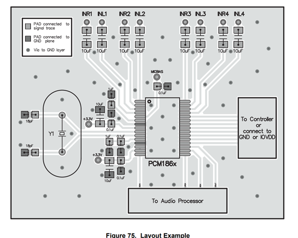
For the voltage divider I am using thin film resistors which should in theory result in a input impedance of approx. 14kOhm together with the ADCs input impedance. I am using a 4 layer board and the second layer is a GND plane below all the paths shown in the pictures.

The ADC is running at 96kHz 32bit setting and I am using some PGA (+3dB) and mixer gain scaling (-8.5dB for balanced) internally.

Can someone give me advice on possibilities how my layout and schematic can be improved regarding EMI and noise coupling?

Any other advices for potential design problems that could be causing the crackling noises?


Help would be much appreciated!

All the best,
Max

  • Hi Max,

    Let me have a look at this and get back to you on this thread in a couple of days.

    Thanks and Regards,

    Lakshmi Narasimhan

  • Hi Lakshmi,

    Thanks, looking forward to your answer!

    Regards,
    Max

  • Hi Max,

    Just wanted to confirm, is there a copper GND pour in the top layer. From the above snapshot, i am only able to see traces connecting the different GND pins, with the decoupling caps connecting to inner GND layers through single vias.

    Also, I would suggest referring to the layout guidelines section in the datasheet, along with the layout example mentioned in the same.

    Thanks and Regards,

    Lakshmi Narasimhan

  • Hello Lakshmi,

    Thanks for your answer.

    No there is no GND copper pour on the top or bottom layers. For signal integrety reasons I always had quite good experience with the approach placing a single GND plane for AGND and DGND on layer 2 and VDD on layer-3 for mixed signal systems. I wanted to avoid "antenna" problems due to copper islands on the top layer.
    Do you think I should consider adding a copper pour on the top layer ?
    For the layout i already tried to stick to the suggested guidelines and example layout.

    In the meantime I could confirm that the noise is induced or at least amplified by radiated EMI from the PSU which is closeby. It seems to be picked up somewhere in the analog front end.

    Do you think it would make sense to put the audio input traces on the back layer ? I need to keep all components on the top layer but I could route the signal lines on layer 4 so there is two solid copper planes (layer 2+3) in between.

    Not sure if it is a good idea to use vias to bring the signal forth and back between the layers, but maybe not to critical with tha analog signals ?

    Best regards,
    Max

  • Hi Max,

    In the meantime I could confirm that the noise is induced or at least amplified by radiated EMI from the PSU which is closeby. It seems to be picked up somewhere in the analog front end.

    For my understanding, was it basically the noise improving/degrading based on whether or not the nearby instrument is moved closer/farther away from the PCB?

    Additionally, I also see that there is a R4-C6-R5 filter at the analog input, and it is 47Ohm-10nF-47Ohm. Does increasing the R4-R5 resistances (or increasing C6) to decrease the cut-off frequency of this filter help?

    Thanks and Regards,

    Lakshmi Narasimhan