This thread has been locked.

If you have a related question, please click the "Ask a related question" button in the top right corner. The newly created question will be automatically linked to this question.

TPA3112D1: TPA3112D1PWPR

Part Number: TPA3112D1

Tool/software:

Hi Team,

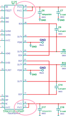
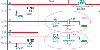
For my new design, I intend to use the TPA3112D1PWPR Mono Class-D Audio Power Amplifier.

A Class-D differential speaker out that delivers 800 mW at 8 ohms from the CPU will serve as the power amplifier's input.

The voltage that will be applied to the TPA3112D1PWPR is 12V. Kindly review the specifications, provide feedback, and verify the attached schematics.

Regards,
Chithraj S

TPA3112D1PWPR.pdf

  • Hey Chithraj, 

    Here are my comments on the schematic:

    • I would pair PVCC pins 16 and 15 together and pair PVCC pins 27 and 28. They should have separate decoupling caps on them to. You would find an example of this in the EVM UG. I have an image below for guide.
    • If the output terminals are going to a SPK, you can add LC-filter decoupling caps. Same for the ferrite bead and same for the inductor.
    • The cap in series to the speaker input terminal is an okay choice. This would block and DC voltage making its way to the speaker.
    • INN and INP need AC caps.
    • Make sure you are using the recommended voltage limits for the SD, GAIN0, GAIN1, and FAULT pins.
    • 100K on AVCC would not allow easy current flow into the device. Use a 10Ohm resistor if possible.

    The EVM UG has a perfect example of how to configure TPA3112D1. 

    -------------------------------------

    images:

    how to tie PVCC lines.

    I hope this was helpful and informative.

    Regards,

    Ore.

  • Hello Ore,

    Thank you for providing the EVM user manual and the thorough review.

    Decoupling caps, designated C480, C481, C482, and C483 in the schematics, are placed separately for pins 15, 16, 27, and 28.

    This will be taken into account when designing the PCB.

    According to the EVM schematics, the GAIN0 and GAIN1 pin voltages are limited by 100K.

    Moreover, the MCU will control the GAIN0 and GAIN1 pins.

    When the amplifier is fully turned off with a low at the SD pin, could you please confirm the current consumption?

    Regards,
    Chithraj S

  • Hey Chithraj, 

    Here are my comments:

    • Another idea recommended for good audio performance from our EVM are snubbers. I have attached an image below.
    • R1 and R2 are 100K pull up resistors to PVCC. This combination provides a small current sink to the GAIN pins. An MCU should be able to control these pins as long the input signal meet the voltage and current requirements. Find images below.
    • Using the SD pin, the current consumption is 400uA according to the DS.


    ----------------------------------------------------------------

    Images:

    current and voltage requirements for GAIN pins.

    snubbers

    I hope this response was informative and helpful.

    Regards,

    Ore.

  • Hello Ore,

    Thank you for the recommendations.

    I'll utilize the same in my design.

    I want to thank you again for your invaluable assistance.

    Regards,
    Chithraj S

  • Thanks. This thread is closed. 

    Regards,

    Ore.