This thread has been locked.

If you have a related question, please click the "Ask a related question" button in the top right corner. The newly created question will be automatically linked to this question.

TLV320AIC3204: Clocks in TLV320AIC3204

Part Number: TLV320AIC3204

Tool/software:

Hello Everyone,

I am working on a project that involves TLV320aic3204 codec. I am confusing below given two: Can anyone Clarify ?

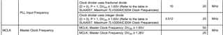
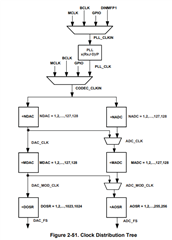
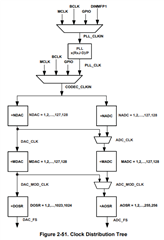
1. The required internal clock of the TLV320AIC3204 can be derived from multiple sources, including the
MCLK pin, the BCLK pin, the GPIO pin or the output of the internal PLL, where the input to the PLL again
can be derived from the MCLK pin, the BCLK or GPIO pins. Although using the PLL ensures the
availability of a suitable clock signal, it is not recommended for the lowest power settings. The PLL is
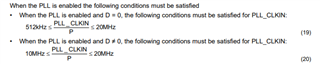
highly programmable and can accept available input clocks in the range of 512kHz to 50MHz.

2.The PLL input supports clocks varying from 512kHz to 20MHz and is register programmable to enable
generation of required sampling rates with fine resolution. The PLL can be turned on by writing to Page 0,
Register 5, D(7).

Can Anyone clarify above two red marked statements. I read that statements in the given aplication reference manual: www.tij.co.jp/.../slaa557.pdf

Thank you in advance

  • Hi,

    Today is a holiday for our team in the U.S. We will follow up with you on Tuesday.

    Thank you for your patience,
    Jeff McPherson

  • Hi,

    It looks like CODEC_CLKIN is rated up to 50MHz or (much) higher with a higher DVdd. CODEC_CLKIN is the clock at the output of the PLL, or the clock that the dividers to get the DAC and ADC clocks come from.

    The PLL input clock is rated up to 20MHz AFTER the P divider. You can think of the PLL clock tree with one block before the PLL of a divider by P, then that clock would be limited to 20MHz. You can see that the rating in the datasheet of the PLL input frequency is with P=1. P can range from 1-8, so really the maximum PLL input clock would be 8 * 20MHz = 160MHz with appropriate P divider value.

    All these images are the relevant tables I found in the datasheet + application reference guide, I hope it helps.

    Let me know if you need more help configuring the PLL or clock tree!

    Best,
    Mir

  • Thank you Mir,

    Can you give

  • Thank you Mir,

    Can you give a basic overview of how the pll clock and other section clocks are configured from the clock tree.

  • Hi,

    As seen in Figure 2-51 in the application reference guide, here is the clock tree. It is read top to bottom. The trapezoid shapes denote a multiplexer, where the user can specify which clock is chosen for the input to that section of the tree. Each of the sections of the tree are configurable with I2C. So, we start by choosing the input clock to the PLL, which could come from MCLK, BCLK, GPIO, or DIN/MFP1. Then, the PLL multiplies up this input clock by a factor of R * J.D / P to generate PLL_CLK. Then the CODEC_CLKIN mux can choose the PLL_CLK as the input to the codec's internal clocks, or you can choose MCLK, BCLK, or GPIO inputs and keep the PLL disabled. CODEC_CLKIN gets passed to the codec clock dividers, which divide by N, then M, then the OSR for the respective DAC or ADC, and there is the option to keep ADC and DAC clocks equivalent as well. OSR is important for any internal processing of the codec, which may need to be as high as 128 for appropriate functionality of the internal filters and other features depending on power and sampling rates chosen. Then, you want the FS to be the sample rate of the device, also called FSYNC or WCLK. All of these dividers and PLL parameters are set with page 0 registers 4-20. Let me know if you have specific questions about this or if you need help with your specific application. 

    Best,
    Mir