This thread has been locked.

If you have a related question, please click the "Ask a related question" button in the top right corner. The newly created question will be automatically linked to this question.

TLV320ADC5140:Currently we want to use this ADC to capture audio, but we can't output the sound

Part Number: TLV320ADC5140

Tool/software:

目前我们想使用 STM32来控制 adc5140进行音频捕获,但是我们的 ADC 似乎无法正常工作,这是我们为这个 ADC 配置的寄存器。

ADC_DATE_INPUT(0x00,0x00);/*选择寄存器的页码*/
ADC_DATE_INPUT(0x02 , 0x81);/*上电*/
ADC_DATE_INPUT(0x05 , 0x05);
ADC_DATE_INPUT(0x07 , 0x40);/*ASI_CFG0 registery音频输出配置*/
ADC_DATE_INPUT(0x08 , 0x20);/*ASI_CFG1 registery音频输出配置*/
ADC_DATE_INPUT(0x09 , 0x00);/*ASI_CFG2 registery音频输出配置*/
ADC_DATE_INPUT(0x0B , 0x00);/*ASI_CH1 registery音频输出配置*/

ADC_DATE_INPUT(0x13 , 0x02);/*设备配置为 从模式,并且时钟信号(BCLK 和 FSYNC)由外部 MCU 生成*/
adc_write_reg(0x14, 0x48);/* 配置采样率,48KHZ */
ADC_DATE_INPUT(0x16 , 0x08);/*MCLK(GPIO 或 GPIx)用作音频根时钟源(MCLK 与 FSYNC 的比率根据 MCLK_RATIO_SEL 设置而定)*/

ADC_DATE_INPUT(0x21 , 0x00);/*禁用输入端GPIO功能*/
ADC_DATE_INPUT(0x22 , 0x00);/*禁用输入端GPI/O功能*/
ADC_DATE_INPUT(0x23 , 0x00);/*禁用输入端GPI/O功能*/
ADC_DATE_INPUT(0x24 , 0x00);/*禁用输入端GPI/O功能*/
ADC_DATE_INPUT(0x25 , 0x00);/*禁用输入端GPI/O功能*/
ADC_DATE_INPUT(0x2B , 0x00);/*禁用输入端GPI/O功能*/
ADC_DATE_INPUT(0x2C , 0x00);/*禁用输入端GPI/O功能*/
ADC_DATE_INPUT(0x3B , 0x00);/*VREF设置为2.75 V,麦克风偏置为3.3*/

adc_write_reg(0x3C,0x20);
adc_write_reg(0x3D,0x60);
adc_write_reg(0x3E,0xC9);
adc_write_reg(0x3F,0x80);
adc_write_reg(0x40,0x00);

adc_CHx_CFGx(CH2_CFG0,0x20);
adc_CHx_CFGx(CH2_CFG1,0x60);
adc_CHx_CFGx(CH2_CFG2,0xC9);
adc_CHx_CFGx(CH2_CFG3,0x80);
adc_CHx_CFGx(CH2_CFG4,0x00);

adc_CHx_CFGx(CH3_CFG0,0x20);
adc_CHx_CFGx(CH3_CFG1,0x60);
adc_CHx_CFGx(CH3_CFG2,0xC9);
adc_CHx_CFGx(CH3_CFG3,0x80);
adc_CHx_CFGx(CH3_CFG4,0x00);

adc_CHx_CFGx(CH4_CFG0,0x20);
adc_CHx_CFGx(CH4_CFG1,0x60);
adc_CHx_CFGx(CH4_CFG2,0xC9);
adc_CHx_CFGx(CH4_CFG3,0x80);
adc_CHx_CFGx(CH4_CFG4,0x00);

adc_write_reg(0x6B,0x00);

adc_write_reg(0x73, 0xF0);IN_CH_EN寄存器
adc_write_reg(0x74, 0xF0);ASI_OUT_CH_EN 寄存器
adc_write_reg(0x75, 0xF4);PWR_CFG 注册


同时我们读取以下三个 registers 的状态:
寄存器地址:ASI_STS , 寄存器状态:ff
注册地址:DEV_STS0 , 注册状态:0
寄存器地址:DEV_STS1 , 寄存器状态:c0
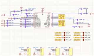
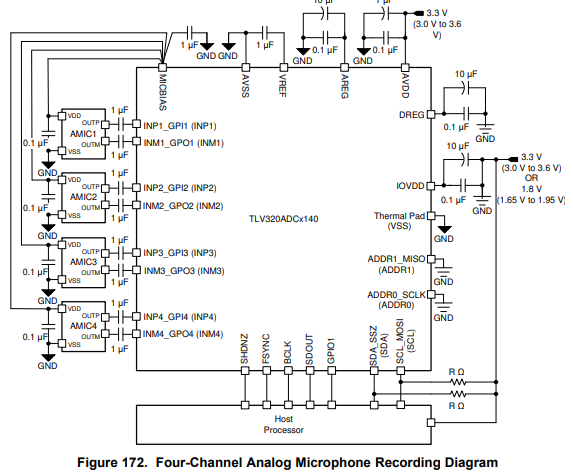
这是我们针对此 ADC 的电路设计原理图

  • What should I do now? Please help me, thank you very much.

  • Hi,

    Couple of things:

    1) Please refer to application section in datasheet for recommended device decoupling.

    2) Please confirm whether in the STM controller, I2S is operating in full-duplex or simplex mode, and which of the I2S_SD and I2Sext_SD is configured as transmitter/receiver.

    Thanks and Regards,

    Lakshmi Narasimhan

  • 1. We replaced the capacitors around the device, but those three registers still read FF,0,C0.
    2.I2S is working in half duplex mode, ADC5140 sends data, STM32 receives data, current configuration is STM32 configured as master, ADC5140 as slave.

    Is there another solution?Thanks and Regards.

  • Hi,

    (1) I am assuming that the ASI_STS register is reading 0xFF while the STM master is active? If so, the register reading back 0xFF is indicating that the ADC is not receiving a valid BCLK and FSYNC. I am seeing that the IOVDD is 3.3V to the ADC, can you confirm that the SCK, WS signals from STM to the ADC are also at the 3.3V IO level?

    Thanks and Regards,

    Lakshmi Narasimhan

  • Hi, I can confirm that these signals are 3.3V levels. I have now tweaked the rest of the program a bit and also reworked the registers. The three registers of the ADC now show the contents at runtime:
    ASI_STS Register content: 42
    DEV_STS0 Register: f0
    DEV_STS1 Register: e0.
    The configuration of the registers after my modification is as follows, please help me to see if there is any error?

    I am only using channel 3 to receive data from the microphone.

    adc_write_reg(ADCX140_PAGE_SELECT,0x00);
    
    adc_write_reg(ADCX140_SW_RESET,0x00);
    adc_write_reg(ADCX140_SLEEP_CFG,0x81);
    adc_write_reg(ADCX140_SHDN_CFG,0x08);
    adc_write_reg(ADCX140_ASI_CFG0,0x40);
    adc_write_reg(ADCX140_ASI_CFG1,0x00);
    adc_write_reg(ADCX140_ASI_CFG2,0x00);
    	
    adc_write_reg(ADCX140_MST_CFG0,0x02);
    adc_write_reg(ADCX140_MST_CFG1,0x40);
    		
    adc_write_reg(ADCX140_CLK_SRC,0x10);
    
    adc_write_reg(ADCX140_INT_CFG,0x00);
    
    adc_write_reg(ADCX140_BIAS_CFG,0x00);
    		
    adc_write_reg(ADCX140_CH1_CFG0,0x20);
    adc_write_reg(ADCX140_CH1_CFG1,0x00);
    adc_write_reg(ADCX140_CH1_CFG2,0xc9);
    adc_write_reg(ADCX140_CH1_CFG3,0x80);
    adc_write_reg(ADCX140_CH1_CFG4,0x00);
    		
    adc_write_reg(ADCX140_CH2_CFG0,0x20);
    adc_write_reg(ADCX140_CH2_CFG1,0x00);
    adc_write_reg(ADCX140_CH2_CFG2,0xc9);
    adc_write_reg(ADCX140_CH2_CFG3,0x80);
    adc_write_reg(ADCX140_CH2_CFG4,0x00);
    		
    adc_write_reg(ADCX140_CH3_CFG0,0x60);
    adc_write_reg(ADCX140_CH3_CFG1,0x00);
    adc_write_reg(ADCX140_CH3_CFG2,0xc9);
    adc_write_reg(ADCX140_CH3_CFG3,0x80);
    adc_write_reg(ADCX140_CH3_CFG4,0x00);
    adc_write_reg(ADCX140_CH4_CFG0,0x60);
    adc_write_reg(ADCX140_CH4_CFG1,0x00);
    adc_write_reg(ADCX140_CH4_CFG2,0xc9);
    adc_write_reg(ADCX140_CH4_CFG3,0x80);
    adc_write_reg(ADCX140_CH4_CFG4,0x00);
    		
    adc_write_reg(ADCX140_DSP_CFG0,0x01);
    adc_write_reg(ADCX140_DSP_CFG1,0x40);
    adc_write_reg(ADCX140_DRE_CFG0,0x7b);
    adc_write_reg(ADCX140_AGC_CFG0,0xe7);
    adc_write_reg(ADCX140_IN_CH_EN,0xf0);
    adc_write_reg(ADCX140_ASI_OUT_CH_EN,0x20);
    adc_write_reg(ADCX140_PWR_CFG,0x40);


  • I'm sorry. I misread that SCK and WS are working at 1.6V, is there something wrong?Thanks and Regards.

  • Hi,

    Sorry for the confusion, so the SCK and WS are working at 1.6V instead of 3.3V? Because the IOVDD is 3.3V, and the digital inputs need to be per the VIH/VIL specifications on the datasheet.

    Additionally, since device is in I2S, and Channel 3 is being used for sending data, we can do the following:

    Configure ASI_CH3 register to give CH3 data on left/right slot 0.

    Thanks and Regards,

    Lakshmi Narasimhan

  • What should I set the voltage of SCK and WS to? How was this set up?

  • I have another question, does IN2P_GPI2 correspond to channel 2? Similarly, does IN12P_GPI1 correspond to channel 1?, Does IN3P_GPI3 correspond to channel 3?, Does IN4P_GPI4 correspond to channel 4?I'm using an analog single-ended input.But now the SDOUT pin output is always 0.Thanks and Regards.

  • Hi Ye,

    Yes your clocks should be set to 3.3V. This is because the logic thresholds are proportional to IOVDD according to the table that Lakshmi shared. Your IOVDD is 3.3V so your clocks must follow.

    Yes the first digit in the pin name corresponds to the channel name as you described.

    You may not be getting any output because your clock voltage is incorrect. Please fix the clock level and see if there's any change.

    Best regards,
    Jeff McPherson

  • Hi Jeff, how should I modify this clock level? Is it necessary to rework the board? Is it possible to get the correct voltage by adding a pull-up resistor on the pins SCK and WS?We currently do not have any resistors connected to these two pins.Thanks and Regards.

  • Hi Ye,

    You would need to check if the STM controller used for the I2S communication is capable of providing I2S signals with 3.3V IO logic, and it would be specific to the microcontroller configurations.

    If it is not, then we may need to either:

    1) Use a level translator to translate the IO levels to 3.3V, or

    2) Use 1.8V as the IOVDD for the ADC (if the I2S signals from the controller are of 1.8V IO)

    Thanks and Regards,

    Lakshmi Narasimhan