This thread has been locked.

If you have a related question, please click the "Ask a related question" button in the top right corner. The newly created question will be automatically linked to this question.

TAS2563: Limit power consumption on non-battery external boost

Part Number: TAS2563

Tool/software:

Hello,

I'm working with TAS2563 on a device that has DC input (not battery). We are using external boost configuration (since we have +12v rail). I'd like to know possible ways to limit the power consumption of the amp. Here are my questions:

  • Is there a way to check if the amp is configured properly to use external boost? I currently have the 'boost enable' unchecked and boost mode = always off.
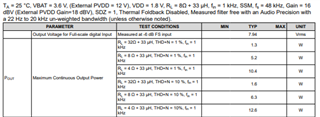
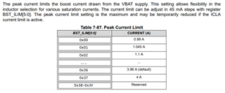
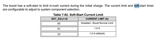
  • The 'peak current limit' under 'channel gain'. Is this acting on the output (to speaker) or input? and does it still work on external boost (mode = always off)? If it's limiter on output, would that mean that the voltage will be the same as PVDD (in this case +12v)?
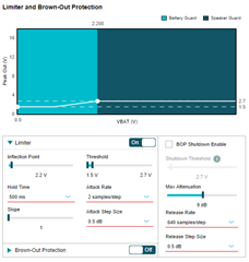
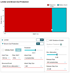
  • Can we somehow use the VBAT battery tracker and Brown-Out Protection on non-battery powered device (to limit peak consumption of amp when total consumption of the device is high)?
  • Any other tips to manage power consumption?
  • Is there a way to import EQ values from external file (e.g csv)?

Thanks in advance!

  • Hey Steve, 

    Here are my comments:

    • For boost to be disabled and always off, TAS2563 would have to be in external PVDD mode. Find more info in this PDF.
    • You could always read the register used to disable boost. "w 98 33 c4" would become "r 98 33 c4". This function applies to all registers.
    • If boost is being provided externally, it's up to the external source to set the current drawn. Peak current limit feature is meant for current pulled from VBAT when internal boost mode is in use. It seems you are using the external PVDD mode for the boost function. These functions affect the output of the IC going into the speaker terminals.
    • The battery tracker/BOP features kick in if the VBAT supply dips below a configured threshold. Whatever source used to power the VBAT pin could experience dips in voltage, this feature is used to protect the IC from these events.
    • Asides from reducing the gain, there's the auto mute feature that also saves power.
    • This end system integration pdf is a perfect guide for importing registers.

    Regards,

    Ore.

  • Hi,

    thanks for the answers! Some follow up question:

    I've been seeing the chip draws power up to 20W under very short time (is this normal?), at the beginning of full-range signal playback. This is unfortunately above the budget that we have for the product, hence the pursue for some kind of limiter. We are using external boost (PVDD) configuration (both in FW and HW) to optimize efficiency since we have +12V rail available and require at most 10W output for the speaker.

    So based on your answer, it looks like there is no way to provide current limit on external boost mode? However, I found in datasheet (section 7.4.3.6) that the chip can monitor PVDD as well. Register names are mentioned (LIMP_ATK_RT[2:0]. etc.) but no further explanation exist. Anyone know if these parameters can actually be used?

    Regards,
    Steve

  • Hey Steve, 

    20W of power is huge for this IC . Ideally you should get around 12W of power on an 4Ohm load. Checkout the DS output power rating:

    What load is being used on your setup?

    Regards,
    Ore.

  • The speaker being used is rated at 4 ohm. It was chosen to utilize the whole capability of the amp.

    From datasheet: "10W peak power into 4Ω load in boost bypass mode using external 12V supply"

  • Hey Steve, 

    this register setting in the image above should allow you control the output current and hence the power. This is in non-bypass mode, so pvdd would be boosted from vbat.. I suggest reducing the current to values the DS supports in internal PVDD mode for safe operation. 20W doesnt sound like safe sustainable operation for this IC.

    There's also a soft start feature that you could use 

    find page 57 of the DS. 

    To get a safe operating output current, use the following steps:

    • p=(Vrms^2) / R
    • retrieve Vrms and R from here to calculate Iout. Highest power from this device is 12.6W on 4Ohm load.

    Regards,
    Ore.

  • Hi Ore,

    12.6W output on 4ohm load would only be feasible if bypass (external PVDD) mode is used, right?

    "The Class-D amplifier is capable of delivering 6.1W of peak power into a 4Ω load at battery voltage of 3.6V using the integrated 11.5V Class-H boost, or 10W peak power into 4Ω load in boost bypass mode using external 12V supply"

    Regards,
    Steve

  • Hey Steve,

    To answer your question, 12.6W is ideal on 4Ohm load depending on the gain configuration and the spec table I provided earlier shows that.

    TAS2563 would be ideal for your setup when working with the 12V rail in your system on this IC. You can get approximately 10W of output power on 4Ohm load by limiting gain settings which inherently limits output current. 

    10W across 4Ohm means about 6.32Vrms which is about 8.9Vpk using the Vrms = sqrt (PR) formula. Checkout this register setting of 8.92Vpk. This setting has enough headroom to avoid clipping. 

    To address current consumption, if in ext. PVDD mode, PVDD would take the bulk of the amount of current used. Using BOP which also works in ext. PVDD mode is to allow for continuous playback when VBAT sags below a certain configurable threshold voltage due to transient current pulls on the output (PVDD line or output terminals). The PVDD thresholds are configurable too and this ultimately controls the current consumption on the device. Once threshold is hit maybe from a surge event that increases gain momentarily, the gain of the output reduces and continues playback. This feature is as a form of protection.

    Parameters of this feature can be controlled. Read the section "7.4.3.6 Supply Tracking Limiters with Brown Out Prevention" for more info. There's a PVDD limiter and a VBAT limiter that can help manage power, and there are thresholds that are configurable for both power lines. These parameters (like the LIMP_ATK_RT[2:0]. etc example you've mentioned in a previous thread) work in ext. PVDD mode that your setup requires. I have tried this out on a setup I have here. This BOP feature is very different from the peak current parameter that I mentioned earlier which seems to work for when VBAT is not in bypass mode, and VBAT is the main channel source of the output current. 

    Checkout the limiter feature in PPC3. Take VBAT=3.8V and PVDD=5V for example:

    Here in limiter settings, 2.2V inflection on VBAT is fine because VBAT is higher than this value, but 2.7V threshold on PVDD would produce an attenuated signal because PVDD is above limit. Current is also reduced in this state.

    Here in BOP settings, if VBAT is below this 4.6V threshold, gain is attenuated and hence current reduces.

    Both features can be on or off and work independently. 

    While you are here, please share your end application.

    Regards,

    Ore.

  • Thanks for the examples Ore!

    I think now I understand more about the BOP and limiter feature. Regarding use case, the product is powered by PoE (48v) with internal converters to lower voltages (12V, 3.3V, etc.). The product got killed by the PoE switch since it draws more power than it is allowed (when playing loud signals at max gain). We know this for sure since the products runs fine if we supply it with a non-limited DC power.

    I have some follow-up questions:

    • The 'AMP_LEVEL' param: is it acting purely as gain (with some mapped peak output voltage) or is it actually a limiter (not affecting the gain)?
    • Can you confirm, that the limiter function inputs data on VBAT and alters/limit the peak out voltage (not actually monitor PVDD)? I guess the assumption here is that both PVDD and VBAT originate from the same rail and hence VBAT can be used as indicator when limiter needs to act?

    It looks to me that at the moment, these limiters functions are great but not an option. In our case (without introducing special circuitry to VBAT), when VBAT dips, the PoE switch has decided to kill the device while the smart amp just get informed through the dipping voltage.

    Do i miss any details? and do you have any other recommendation?

    Regards,
    Steve

  • Hey Steve, 

    "Amp level" is purely gain. If BOP and limiter are not functional, the amp level at the output would be whatever you set here. 

    The limiter can use data from vbat but not change vbat. What it would change is the PVDD voltage the device needs based on the i2c configuration. PVDD is really the output headroom voltage. VBAT and PVDD are separate rails and both need to be biased separately to make the IC work especially in bypass/external pvdd mode. Seeing as your application isn't battery powered, my setup (using a PSU) wasn't as well. VBAT was below a threshold the limiter was supposed to respond to and I got a continuous attenuated output. This could apply to your setup. Also, the attenuation can be configured, the image I provided shows an attenuation of 9dB on the output signal.

    The limiter option that reduces gain based on vbat can be configured in a particular way with respect to VBAT. In ext. pvdd mode, VBAT would pull less current and current requirements would be loaded on PVDD and not VBAT. These rails are not shared. Only circuitry needed on vbat is decoupling. Check the EVM UG for tas2563. BTW this applies to both TAS2563YBG and TAS2563RPP packages.

    Regards,
    Ore.