This thread has been locked.

If you have a related question, please click the "Ask a related question" button in the top right corner. The newly created question will be automatically linked to this question.

TAS5548:Tas5548

Part Number: TAS5548
Other Parts Discussed in Thread: PCM1808

Tool/software:

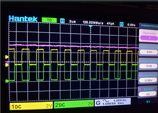
Best regards, I'm using the tas5548 evaluation board, but I'm getting noise at the output, the master volume is set to +17.75db, but in the datasheet 7.4.17 THD manager session they mention about the pre and post, if I disable them it generates a lot of noise at maximum volume, but if I adjust the post to -36db it decreases the noise,  but the volume of output decreases, I hope for your help. 

  • Hi Teobaldo,

    What is the input signal amplitude you're using? Also, what are the specific gain levels you're setting for the device?
    We'll double check on our side based on this information.

    Best regards,
    -Ivan Salazar
    Applications Engineer

  • no more than 120mv, I'm using the PCM1808, the logs are sent via the esp32..

    #include <Wire.h>
    
    #define TAS5548_ADDR 0x1A  // Dirección I2C del TAS5548
    
    void writeReg(uint8_t reg, uint8_t val) {
      Wire.beginTransmission(TAS5548_ADDR);
      Wire.write(reg);
      Wire.write(val);
      Wire.endTransmission();
    }
    
    void writeReg4(uint8_t reg, uint8_t b0, uint8_t b1, uint8_t b2, uint8_t b3) {
      Wire.beginTransmission(TAS5548_ADDR);
      Wire.write(reg);
      Wire.write(b0);
      Wire.write(b1);
      Wire.write(b2);
      Wire.write(b3);
      Wire.endTransmission();
    }
    
    void setup() {
      Wire.begin(21, 22); // SDA, SCL
      delay(500);
    
      // ==== Configuración inicial del TAS5548 ====
      writeReg(0x03, 0xA0); // PWM high pass activado, MidZ habilitado, canales activos
      writeReg(0x04, 0x03); // SDOUT activo
      writeReg(0x0E, 0x14); // I2S, 24 bits
      writeReg(0x0F, 0x00); // Mute suave desactivado
      writeReg(0x10, 0x0A); // Energy manager
      writeReg(0x14, 0x01); // Umbral de automute -60dBFS
      writeReg(0x15, 0x00); // PWM min threshold
      writeReg(0x16, 0x01); // Modulación 98.43% CH1/2
      writeReg(0x17, 0x01); // Modulación 98.43% CH3/4
      writeReg(0x24, 0x0F);  // Tiempo de secuencia PWM
      writeReg(0x25, 0x00);  // BD Mode (D5 = 0)
    
      // ==== Configurar BD Mode en canales ====
      writeReg(0x30, 0x11); // CH1/CH2 en BD
      writeReg(0x31, 0x11); // CH3/CH4 en BD
    
      // ==== Asignación de canales a salidas PWM ====
      writeReg(0x34, 0x01);  // PWM1 = canal 1, PWM2 = canal 2
      writeReg(0x35, 0x23);  // PWM3 = canal 3, PWM4 = canal 4
    
      // ==== Enrutamiento SDIN1 a canales ====
      writeReg(0x36, 0x00); // Canal 1 → SDIN1
      writeReg(0x37, 0x00); // Canal 2 → SDIN1
      writeReg(0x38, 0x00); // Canal 3 → SDIN1
      writeReg(0x39, 0x00); // Canal 4 → SDIN1


      // ==== Retardo entre canales (si se desea) ====
      writeReg(0x38, 0x10);  // Canal 0: +16 DCLK
      writeReg(0x39, 0x10);  // Canal 1: +16 DCLK
      writeReg(0x3A, 0x10);  // Canal 2: +16 DCLK
      writeReg(0x3B, 0x10);  // Canal 3: +16 DCLK
    
      // ==== Volumen maestro ====
      writeReg4(0xD9, 0x00, 0x00, 0x00, 0x01); // +17.75 dB
      //writeReg4(0xD9, 0x00, 0x00, 0x00, 0x0C); // +15dB
    
      // ==== THD Manager ====
      //writeReg4(0xE9, 0x03, 0x80, 0x00, 0x00); // THD Pre +20 dB
      writeReg4(0xE9, 0x03, 0x40, 0x00, 0x00); // THD Pre +17 dB
      writeReg4(0xEA, 0x00, 0x08, 0x00, 0x00); // THD Post -36 dB
    
      // ==== Configuración de umbrales alto y bajo para los canales ====
      // Umbral alto para satélite (en formato 5.23
      writeReg4(0xBB, 0x00, 0x00, 0x1F, 0x40);  // 1.5 
      // Umbral bajo para satélite (en formato 5.23
      writeReg4(0xBC, 0x00, 0x00, 0x10, 0x00);  // 1.0 
      // Umbral alto para subwoofer (en formato 5.23
      writeReg4(0xBD, 0x00, 0x00, 0x20, 0x00);  // 2.0 
      // Umbral bajo para subwoofer (en formato 5.23
      writeReg4(0xBE, 0x00, 0x00, 0x10, 0x00);  // 1.0 
    }
    
    void loop() {
      // Lógica opcional
    }

  • Thanks for the additional information, we'll go through it and get back with further comments later this week.

    Best regards,
    -Ivan Salazar
    Applications Engineer

  • Best regards, it's been 10 days, no help

  • Hi Teobaldo,

    Sorry for the delay.

    I've gone through your script and note a few things below:

    • register 0x0e is set to 0x14, but based on the in-line comments it says "I2S, 24bits" so you may use the default value of 0x55 instead
    • register 0x14 is set to 0x01 which is threshold of -90dBFS but your in-line comment says "-60dBFS", just wanted to double check which you expect
    • register 0x16 is setting different modulation indexes for CH1 and CH2, note that MSB corresponds to CH2 and LSB to CH1
    • register 0x17 has same concerns as above 0x16
    • register 0x31 is setting the same input mux settings for CH3 and CH4 as of CH1 and CH2, also all 4 select channel 2, just wanted to double check this is as expected
    • there is a section for register 0x36, 0x37, 0x38 and 0x39 with some reference to SDIN1, note that these registers are used for other purposes so this section may be incorrect
    • registers 0x38, 0x39, 0x3a and 0x3b are all set to the same value. Based on the description from section 7.6.2.19 having a different delay for each channel may help reduce THD due to PSU overload or channel intermodulation. May be good idea testing with the default values.

    Other than that, it may be a good idea to start using most of default settings and only add minor changes in settings at a time, starting with THD manager as this feature may introduce clipping which will affect THD performance.

    Best regards,
    -Ivan Salazar
    Applications Engineer

  • The default setting refers to those in: 7.6 Register Maps?

  • I was looking in the datasheet, but I didn't find any information about the dead point, since the PWM outputs + and - are not offset.

  • Yes those from reg map; these should be the same as the content of the device memory after power cycle.

    Best regards,
    -Ivan Salazar
    Applications Engineer