This thread has been locked.

If you have a related question, please click the "Ask a related question" button in the top right corner. The newly created question will be automatically linked to this question.

TAS3251: Problems with PBTL Mode

Part Number: TAS3251
Other Parts Discussed in Thread: PCM1863

Tool/software:

Hello E2E Experts,

Good day.

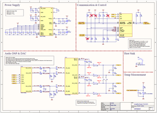
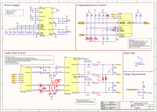
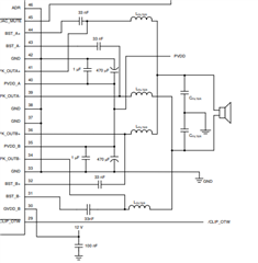
My Project contains 1x PCM1863 as audio source and 2x TAS3251 to realize 2.1 audio system. The PCM1863 Audio Input and one TAS3251 in BTL 2.0 Mode is working fine. The TAS3251 device in PBTL mode for subwoofers has no pwm output signals. The I2S signal is complete and correct and the clock is configured correctly. No errors are reported by FAULT pin, Clip OTW pin and fault register 0x5E and 0x5F (both = 0x0). The mode pin has 3V3 level and the SPK_INB+ and - are connected to GND via 0R resistor. The device in PBTL mode uses same parts as device in BTL mode and is in Post-Filter configuration.

Are there more configurations to do before TAS3251 has an output signal in PBTL mode? Are there additional registers for diagnostics? How can I check if DSP configuration was successful?

Regards,

TICSC

  • Hey,

    Can you send the schematic of this setup?

    Regards,

    Ore.

  • Hello Ore,

    Good day.

    Below are the schematic.

    Regards,

    TI-CSC

  • Hey TI-CSC,

    I have questions:

    • in PBTL mode, is DAC-OUTB not going to SPK-INB?
    • is the customer trying to implement post-filter PBTL or Pre-Filter PBTL? 

    Regards,
    Ore.

  • Hello Ore,

    Good day.

    for the first question:
    - actually I don't know exactly if DAC-OUTB and SPK-INB is working or not, because I don't know how to test. But from my understanding of the datasheet (Page 6, Table 1), the port B should be muted and grounded.
    for the second question
    - my aim was to use post filter PBTL, so I can use same filter parts for BTL and PBTL mode.

    I have the problem, that I don't know what is wrong and there are inconsittencies between datasheet and pure path output for dsp configuration. For example according to the datasheet, the address for swap command is Book 0x8C, Page 0x05, Register 0x7C to 0x7F. The pure path console use Book 0x8C, Page 0x23 Register 0x14 to 0x17 for swap command.
    Do you have a working DSP configuration for the post-filter PBTL mode I can test?

    Regards,

    TICSC

  • Hello,

    I suggest removing the extra cap to GND on the spk B terminals when switching to PBTL mode. 

    Create a circuit to short those caps out for the pbtl mode.

    It seems you are using post-filter method. Try to emulate the cfg provided by DS. 

    Implementing 4 inductors is fine to maintain board space but maybe try to replicate exactly what the PBTL mode is on page 104 of the DS. If you notice, the spare caps you have connected to the output of your schematic are gone compared to the DS suggestion. 

    Checkout the output post-filter PBTL app the DS has:

    Regards,

    Ore.

  • Hello Ore,

    Good day.

    Thank you for the hint. I will try next week. The Capacitors I forgot to remove or better, I wasn't aware.
    Theoretically, the device should work without any manipulation of DSP registers, right?

    Regarding this DSP registers manipulation, my current implementation does not work. The Swap flag in Book 0x8C, Page 0x05, Register 0x7C does not reset after setting it. How can I check, which book and page a currently active? Which registers I have to write to send Swap Flag?

    Regards,

    TICSC

  • Expect a response next week. I am currently OoO.

    Regards, 

    Ore.

  • Hello Ore,

    Good day.

    Just an update - I disassembled the capacitors, but it does not changed the behaviour of the amplifier. 

    Regards,

    TICSC

  • Hey TICSC, 

    For pbtl application, you'll have to use the exact configuration provided by the DS. 

    Which terminals on the output do you have connected to your speaker? 

    Where is PVDD on the output of your schematic in pbtl mode?.

    Regards,

    Ore.

  • Hello Ore,

    Good day.

    I will provide you the complete schematic for amplifier. Than you have all insights to my circuits. Currently I use a 24 V power supply with 3A current limit.

    In addition attached the register values of my both amplifiers I use in a device. Maybe you can find something in it.

    5327.Amplifier.pdf

    Amplifer_0.1_Mode_Register_Book0_Page0.csv

    Amplifer_2.0_Mode_Register_Book0_Page0.csv

    To be sure that the amp is working in general, I tried the amplifier I want to use for PBTL mode, in BTL mode. For this, I removed the solder bridge of the net ties and changed the mode by resistor change. That works fine.
    In PBTL mode, spk_out+ and - were on a voltage level of round about 450mV. In BTL mode, the voltage level of Spk_OutA+ and A- are round aboud 12 V.
    Maybe this information will help you for better diagnostic.

    Regards,

    TICSC

  • Hey TICSC, 

    This is proof your IC is working and not responding in PBTL mode because the PBTL mode you are using is incorrect. The only way the PBTL mode would work on your setup is if you strictly follow the PBTL configurations available on the DS. 

    Do not leave any stray connections or caps that worked in BTL mode in PBTL mode. 

    Pay attention to how all the wires on the output terminal are shorted and crossed to achieve playback mode in this configuration. There is nowhere in the DS that shows that the PBTL mode is dependent on any software I2C writes or particular input configuration.

    This PBTL is all hardware dependent and strictly for the output terminals. You are free to use L and/or R channel digital input, same for analog input. Until this point on the output is reached and correct is when your PBTL mode would work. I see your input is analog, I expect this part to be the same when moving from BTL to PBTL mode. However, this wouldn't apply to the output configuration.  

    Regards,

    Ore.