This thread has been locked.

If you have a related question, please click the "Ask a related question" button in the top right corner. The newly created question will be automatically linked to this question.

TLV320AIC3007: Schematic design check request

Part Number: TLV320AIC3007

Tool/software:

Hi all,

We designed the schematic using the TLV320AIC3007, but in a design refinement it doesn't output audio anymore .

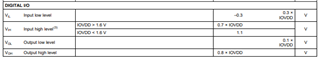
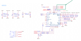
Here's the altered schematic, where SAI5 is a 1.8V level signal.

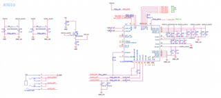
Here's the schematic before this, which uses the SAI2 signal at 3.3V levels. The audio works during debugging, but only when you press the answer button on the headset can you hear the sound clearly.

Can you help check the altered schematic for design errors? What can be changed to make it work.

With best regards.

Xavier

  • Hi Xavier,

    If you are providing an IOVDD of 3.3V, then 1.8V will not be sufficient as a digital HIGH level and so the ASI will not function as expected. In the datasheet, we can see that the input high level minimum is 0.7 x IOVDD, so if your IOVDD is 3.3V that is a minimum digital high of 2.31. So, I would recommend making your IOVDD also 1.8V so that SAI clocks and data are also expected to be at 1.8V.

    Let me know if you have more questions here.

    Best,
    Mir

  • Hi Mir,

    Thanks for the reply.

    In fact, I've tried changing the IOVDD to 1.8V but it doesn't seem to have an effect, could it be a problem with incorrect driver layer changes?

    So,I'm wondering if any of the signals need to be changed other than IOVDD?

    For example, in the latest schematic, I2C4 and SAI3_RXFS are also signaled at a 3.3V level.Do these signals need to be modified?

    Best and regards,

    Xavier

  • Hi Xavier,

    I see, yes, I2C should be pulled up to the IOVDD level of 1.8V, and if you are providing IOVDD of 1.8V, the RESET pin should be HIGH at IOVDD. Let me know if this fixes your issue.

    Best,
    Mir