Tool/software:
Hello
I am trying to set up TLV320ADC3101 as a slave to the i2s bus.
I set BCLK = 1.536 MHz, WCLK = 48 kHz without using MCLK.
The MCU can output BCLK and WCLK without any problem.
However, the DOUT signal is not received.
When I checked with an oscilloscope, it is LOW and there is no change.
The reset pin is set to high, and I use two unbalanced (single-ended) microphones.
Below is a reproduction of the register write.
Am I missing something? Is the register write order wrong?
Was it a mistake not to use MCLK?
Any advice would be greatly appreciated.
--------------------------------------------------------------
TLV320_WriteReg(0x18, 0x00, 0x00); // page 0
TLV320_WriteReg(0x18, 0x01, 0x01); // soft reset
HAL_Delay(50);
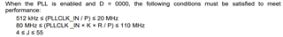
TLV320_WriteReg(0x18, 0x04, 0x07); // PLL_CLKIN = BCLK
TLV320_WriteReg(0x18, 0x05, 0x91); // Enable PLL, P = 1, R = 1
TLV320_WriteReg(0x18, 0x06, 0x08); // J = 8
TLV320_WriteReg(0x18, 0x07, 0x00); // D (MSB)
TLV320_WriteReg(0x18, 0x08, 0x00); // D (LSB)
TLV320_WriteReg(0x18, 0x19, 0x03); // CLKOUT = PLL_CLK
TLV320_WriteReg(0x18, 0x12, 0x81); // NADC = 1, enable
TLV320_WriteReg(0x18, 0x13, 0x81); // MADC = 1, enable
TLV320_WriteReg(0x18, 0x14, 0x80); // AOSR = 128
TLV320_WriteReg(0x18, 0x15, 0x80); // IADC = 128
TLV320_WriteReg(0x18, 0x16, 0x04); // miniDSP decimation = 16
TLV320_WriteReg(0x18, 0x1B, 0x00); // (slave mode, 16bit, BCLK/WCLK in)
TLV320_WriteReg(0x18, 0x1E, 0x00);
TLV320_WriteReg(0x18, 0x3D, 0x01); // Page 0, Reg 0x3D → PRB_R1
TLV320_WriteReg(0x18, 0x0B, 0x81); // NDAC enabled, NDAC = 1
TLV320_WriteReg(0x18, 0x0C, 0x82); // MDAC enabled, MDAC = 2
TLV320_WriteReg(0x18, 0x00, 0x01); // page 1
TLV320_WriteReg(0x18, 0x33, 0x68); // MICBIAS1/2 = 2.5V
TLV320_WriteReg(0x18, 0x34, 0xCF); // Left = IN2L_P, others off
TLV320_WriteReg(0x18, 0x37, 0xCF); // Right = IN2R_P, others off
TLV320_WriteReg(0x18, 0x3B, 0x5F); // Left PGA
TLV320_WriteReg(0x18, 0x3C, 0x5F); // Right PGA
TLV320_WriteReg(0x18, 0x00, 0x00); // page 0
TLV320_WriteReg(0x18, 0x35, 0x10); // DOUT
// ADC Power up
TLV320_WriteReg(0x18, 0x51, 0xC0)
TLV320_WriteReg(0x18, 0x52, 0x00)
TLV320_WriteReg(0x18, 0x54, 0x00)
TLV320_WriteReg(0x18, 0x53, 0x70)
TLV320_WriteReg(0x18, 0x55, 0x70)
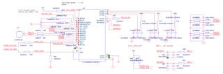
^TLV320ADC3101 circuit
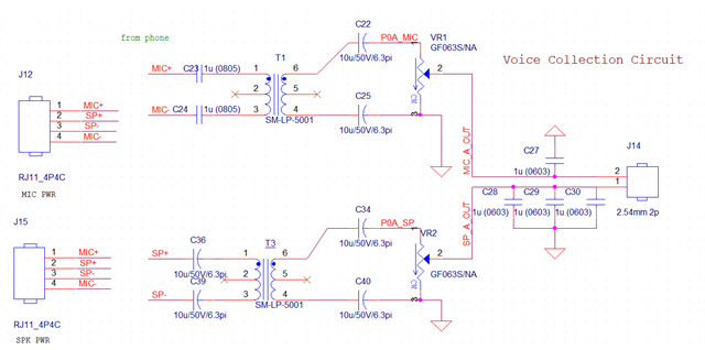
J14 and J17 are connected to each other.