TLV320AIC3100: Inconsistency in MIC PGA Gain

Part Number: TLV320AIC3100

Tool/software:

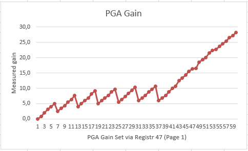
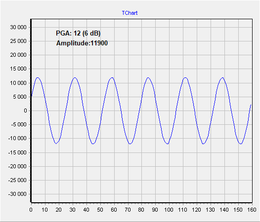
I have encountered an inconsistency in PGA Gain setting. When I gradually increase the value in Page 1 Register 47 the measured gain doesn't increase gradually, but there are drops in gain at some values. Please see included graph.

The drops in gain are at the following Page 1 Register 47 values: 12 (6 dB), 24 (12 dB), 36 (18 dB), 48 (24 dB), 60 (30 dB), 72 (36 dB)

I should note that AGC is switched off.


  • Hi Stanislav,

    This looks like the measurement tool is scaling its range as the input signal increases and might be leading to strange results. 

    Can you give more detail on how this plot was taken? How is the input signal being adjusted to prevent clipping?

    Thanks,
    Jeff McPherson

  • Hi Jeff,

    I can exclude clipping as well as measurement tool scaling. The measurement arrangement is as follows: Analog input MIC1LP is driven by a sine wave from a signal generator. The digital output from audio codec is transferred to a data stream. The data stream is analyzed on PC by special SW, that can draw signal from received data - please see attached file. As you can see, the output digital signal is not clipped. I should note that we use the measurement arrangement for years as we are producer of VoIP communication systems and we use various audio codecs (from Conexant, Wolfson).

    Best regards

    Stanislav

  • Hi Stanislav,

    Understood, thank you.

    I assume as the PGA gain is being increased you are reducing the input signal level? Could you show me on this software 5dB vs 7dB PGA gain, as well as the input signal level given for those two points? This is the first drop off on the original excel plot. I want to understand the conditions around that dip.

    Best regards,
    Jeff McPherson

  • Hi Jeff,

    You are right, we adjust the input signal level when necessary to avoid clipping.

    Here are the measurement values around the "drop gain point (6 dB)":

    Input analog signal amplitude: 500 mV (1 V peak-peak)

    ADC Digital gain (Page 0 Register 83) Value: 0 (0 dB)

    PGA Value:                    Measured digital amplitude:

    8 (4 dB)                          14460

    9 (4.5 dB)                       15484

    10 (5 dB)                        15996

    11 (5.5 dB)                      16764

    12 (6 dB)                         11900

    13 (6.5 dB)                      12412

    14 (7 dB)                         13436

    Notes:

    1. I attach a few output signal graphs. I should note that in the digital data stream path is a G711 mu-law codec that brings a quantization error. Anyway the quantization error is small (in the order of tents dB). 

    2. The graphs are not 100% perfect as they are drawn by connecting the discrete measured values by lines.

    Best regards

    Stanislav


  • Hi Stanislav,

    Thanks for the details. How exactly is the input level turned down as PGA gain increases? Is it 1:1 with the theoretical PGA gain? i.e. when PGA gain is 4dB, input signal is reduced from 1Vpkpk by 4dB? The next best step is to try to recreate this on our end, since it isn't expected from what I can tell.

    Could you share your starting register configuration? Assuming that once the test is going, PGA gain is the only register changed.

    Best regards,
    Jeff McPherson

  • Hi Jeff,

    As I increase PGA gain I keep the input level constant until the moment the output level approach almost the maximum. Then I decrease the input level by 6 dB. Of course for gain calculation I consider the 6 dB decrease.

    Here is the registers configuration (the first value of the pair is register address and the second is written value):

    // PLL and CLOCK setting. MCLK = 3.072 MHz. CODEC_CLKIN = (PLL_CLKIN*R*J.D)/P = (3.072 MHz*16*2.0)/1 = 98.304 MHz.
    // DAC_CLK = DAB_PRB = CODEC_CLKIN/NDAC = 98.30375 MHz/8 = 12.28796875 MHz
    // DAC_MOD_CLK = DAC_CLK/MDAC = 12.28796875/12 = 1.023997396 MHz
    // DAC_fs = DAC_MOD_CLK/DOSR = 1.023997396/128 = 7.999979 kHz
    {0x00,0x00},      /* --- Set Page 0 --- */
    {0x33,0x00},      /* P0/R51(0x33): GPIO1 disabled (input and output buffers powered down) */
    {0x04,0x03},      /* P0/R4(0x04) CODEC_CLKIN = PLL_CLK, PLL_CLKIN = MCLK */
    {0x05,0x10},      /* P0/R5(0x05) PLL divider P=1, PLL multiplier R=16, PLL is powered down */
    {0x06,0x02},      /* P0/R6(0x06) PLL multiplier J=2*/
    {0x07,0x00},      /* P0/R7(0x07) PLL fractional multiplier (MSB) D=0 */
    {0x08,0x00},      /* P0/R8(0x08) PLL fractional multiplier (LSB) */
    {0x0B,0x08},      /* P0/R11(0x0B) DAC NDAC divider N=8. Divider is powered down. */
    {0x0C,0x0C},     /* P0/R12(0x0C) DAC MDAC divider M=12. Divider is powered down.*/
    {0x0D,0x00},      /* P0/R13(0x0D) DOSR MSB (DAC OSR) DAC oversampling = 128 */
    {0x0E,0x80},      /* P0/R14(0x0E) -""- LSB */
    {0x12,0x08},      /* P0/R18(0x12) ADC NADC divider N = 8. Divider is powered down. */
    {0x13,0x0C},      /* P0/R19(0x13) ADC MADC divider M = 12. Divider is powered down. */
    {0x14,0x80},      /* P0/R20(0x14) AOSR (ADC OSR) ADC oversampling = 128 */
    // Power up
    {0x05,0x90},      /* P0/R5(0x05) PLL divider P=1, multiplier R=16, PLL is powered up */
    {0x0B,0x88},      /* P0/R11(0x0B) DAC NDAC divider N=8. Divider is powered up. */
    {0x0C,0x8C},     /* P0/R12(0x0C) DAC MDAC divider M=12. Divider is powered up.*/
    {0x12,0x88},      /* P0/R18(0x12) ADC NADC divider N = 8. Divider is powered up. */
    {0x13,0x8C},      /* P0/R19(0x13) ADC MADC divider M = 12. Divider is powered up. */
    {0x00,0x03},       /* --- Set Page 3 --- */
    {0x10,0x00},       /* P3/R16(0x10): Internal oscillator is used for programable delay timer. */
    // Audio interface setting
    {0x00,0x00},       /* --- Set Page 0 --- */
    {0x1B,0x4C},      /* P0/R27(0x1B): Codec interface control: DSP mode, 16 bits word length, BCLK is output, WCLK is output  */
    {0x1C,0x01},      /* P0/R28(0x1C): Data-Slot Offset = 1 BCLKs */
    {0x1D,0x09},      /* P0/R29(0x1D): DIN-to-DOUT loopback disabled, ADC-to-DAC loopback disabled, BCLK is inverted, BDIV_CLKIN = DAC_MOD_CLK */
    {0x1E,0x04},      /* P0/R30(0x1E): BCLK Divider N = 4, BCLK N-divider is not powered up. */
    {0x1E,0x84},      /* P0/R30(0x1E): BCLK Divider N = 4, BCLK N-divider is powered up. */

    // DAC and speaker setting
    {0x3C,0x01},      /* P0/R60(0x3C): DAC signal-processing block PRB_P1. */
    {0x00,0x01},       /* --- Set Page 1 --- */
    {0x2C,0x00},      /* P1/R44(0x2C): HPL and HPR as headphone drivers, Default DAC mode */

    // ADC and microphone setting
    {0x00,0x00},       /* --- Set Page 0 --- */
    {0x3D,0x04},      /* P0/R61(0x3D): ADC signal-processing block PRB_P4. */
    {0x00,0x01},       /* --- Set Page 1 --- */
    {0x2E,0x00},      /* P1/R46(0x2E): MICBIAS output is powered down, Device software power down is not enabled.  */
    {0x31,0x00},      /* P1/R49(0x31): CM is not selected for the MIC PGA, MIC1LM is not selected for the MIC PGA. */

    // Talk setting 
    {0x00,0x00},      /* --- Set Page 0 --- */
    {0x3F,0x4A},      /* P0/R63(0x3F): R-chan DAC powered up, L-channel DAC data path=off, Right-channel DAC data path=left data, DAC soft-st.disabled */
    {0x40,0x08},      /* P0/R64(0x40): Left-channel DAC muted, Right-channel DAC not muted, Left and right channels have independent volume control. */
    {0x00,0x01},      /* --- Set Page 1 --- */
    {0x23,0x04},      /* P1/R35(0x23): DAC_L is not routed anywhere, DAC_R is routed to the right-channel mixer amplifier, no other routings. */
    {0x1F,0x54},      /* P1/R31(0x1F): HPL output driver is powered down, HPR output driver is powered up, Output common-mode voltage = 1.65 V */
    {0x00,0x00},      /* --- Set Page 0 --- */
    {0x51,0x82},      /* P0/R81(0x51) ADC is powered up, Digital microphone is not enabled, ADC channel volume control soft-stepping is disabled. */
    {0x00,0x01},      /* --- Set Page 1 --- */
    {0x30,0x80},      /* P1/R48(0x30) MIC1LP selected for MIC PGA, RIN = 20 kOhm, MIC1RP,  MIC1LM not selected. */

    The routine for microphone volume control sets the following registers (during the test I keep Digital gain set to 0 dB) :

    {0x00,0x01},                   /* --- Set Page 1 --- */
    {0x2F,MICPGAGain},     /* P1/R47(0x2F): MIC PGA Gain (0 dB...59.5 dB) */
    {0x00,0x00},                  /* --- Set Page 0 --- */
    {0x53,DigitalGain};        /* P0/R83(0x53): ADC Digital Volume Control Coarse Adjust (-12...20 dB) */
    {0x52,0x00};                  /* P0/R82(0x52): ADC Digital volume Fine Adjust (0..-0.4 dB). ADC mute/unmute. */

    Best regards

    Stanislav

  • Hi Stanislav,

    I am going to take over testing this configuration as Jeff is out this week. However, please give me another day or two to recreate this in our lab. Another thought I have here is - is your soft stepping disabled? If you measure too quickly, maybe the steps are ramping between gain levels? I will recreate your measurements soon.

    Best,
    Mir

  • Hi Mir,

    OK.

    The soft stepping is disabled.

    Best regards

    Stanislav

  • Hi,

    Please give me a day or two and I will get back to you on my measurements here. Sorry about the delay.

    -Mir

  • Hi Mir,

    How are things progressing with the measurement?

    Stanislav

  • Hi Stanislav,

    Mir is out of office right now and can get back to this thread next week.

    Best,

    Garret

  • Hi Mir,

    Any progress with measurement? It's been quite a long time since there has been any progress.

    Best regards

    Stanislav
  • Hi, 

    So sorry about the delay I can work more on it this week.

  • Hi Stanislav,

    I was able to test this today and verified what you were seeing - there are jumps in the output dBFS digital "volume" of the input signal. I think there are a few reasons why we are seeing this behavior, and some interesting avenues to explore. 

    My first suggestion is to assign something on the M terminal of the ADC, this is with page 1 register 49 (0x31). When it is set to common mode, we see a 6dB increase in the output dBFS, and the jump at 6dB of gain does not occur anymore. However, we reach full scale a lot sooner, actually around 5 or 6 dB of gain (since it starts at around there). When we change register 83 to the max digital volume reduction on the ADC, -12dB, we still see the jumping in gain when the M terminal is not set, but when it is, we avoid the gain jump but experience distortion around 6dB still. This is likely due to the stage at which this gain reduction happens - the PGA is the first thing that happens to the input before it even goes into the ADC, so if the ADC receives a signal that is too high, it will not be able to decrease it digitally while keeping the distortion down. The distortion occurs when the signal is too big going in to the ADC. We can measure the distortion with a THD measurement. 

    What is interesting to me is the jumps in output THD as compared to the PGA gain when you do not have anything connected to the M terminal happen at these few set values every 6dB of gain, and then after ~42dB, the distortion overtakes the gain error and it finally looks like it is clipping, similar to how my 6dB of gain looked on the input signal when the M terminal was set. I measured THD alongside the dBFS value for many different PGA gain levels and saw that after each "jump" in the gain, the THD got worse by around 5-6dB as well. The gain jumps were around 4-5dB increase from what was expected of the output at those points. From these values being similar, I would guess that internally there are these plateaus of PGA gain, where the signal maybe would clip if it was balanced correctly, but maybe the ADC itself cannot recognize the signal correctly when there is nothing to "compare" on the PGA. Just an idea.

    If you can change that register to set the M terminal to the common mode, and then decrease the analog signal coming in to the device, we can make sure that there are no more strange discrepancies in the PGA gain. But, I think this should solve your problem. Sorry about the delay here again. I am happy to test this more if you need me to.

    Best,
    Mir

  • Hi Mir,

    thank you very much for your answer. I'm a bit confused about THD when M terminal is set to common mode. In the second paragraph you wrote that you experienced distortion about 6dB even when M terminal is set to common mode. Does it only happen when the input signal level is high? If the input signal level is low enough, does THD increase as the PGA Gain value increase?

    Best regards

    Stanislav

  • Hi Stanislav,

    Yes, this was happening because the starting volume at 500mV in like you were using is around -5dBFS. So, when the gain is set near this, we see analog "clipping" in the ADC, which we can measure as higher distortion, since it typically consists of more harmonics of the original sine wave. If the input level was lower, THD+N should stay around the same as the gain value increases. Let me know if you need more help here Slight smile

    Best,
    Mir

  • Hi Mir,

    I understand.

    I tried configuration with M terminal set to common mode. As you mentioned, there aren't "gain jumps" in this case. But in this configuration a DC voltage offset is present in the digital output signal (see image1). The value of the DC voltage offset is depended on PGAGain and Digital gain. The DC voltage offset decreases the maximum output signal span - with increasing input voltage level, the output signal starts to be clipped in the positive half-wave much earlier than in the negative half-wave (see image2; in this case the input signal is a bit noisy, so the wave is not ideal, but the effect is clearly visible). Is there any way how to get rid of the DC voltage offset? Or, at least, is an information available about DC voltage offset value. I didn't find anything in the datasheet. I think this information is quite important as the DC voltage offset in fact reduces the overall achievable gain.

    Best regards

    Stanislav

  • Hi,

    Can you provide your register settings? We expect there to be some bias on the signal, since the input cannot go below 0V, there are AC-coupling capacitors on the input to allow there to be an internal bias. I believe by using VCOM as the (-) side of the PGA, we take the difference between the input that should be centered around 0 after a decoupling capacitor, and the common mode so that there will always be a common mode/bias on the output into the ADC. I believe it is the same common mode as the headphone common mode, set with page 1 register 31. If you adjust that register do you see the DC offset change?

    -Mir

  • Hi Mir,

    1) The register settings is the same as I send you on Jul 21, except:

    P1/R49 = 0x80;

    P1/R47 (MIC PGA Gain), P0/R38 (ADC Digital volume) - these registers were set according to the values written on the graph (please zoom the graphs I last send you).

    2) It doesn't seem that the common mode is the same as the headphone common mode. When I change headphone common mode (P1/R31) there is no change in the DC voltage offset.

    3) I have measured how the DC voltage offset depends on the PGA Gain setting. Here are the results:

    PGA Gain:       Digital DC Voltage offset:

    0 db                  604

    5 dB                 1052

    10 dB               1244

    15 dB               1340

    20 dB               1308

    25 dB               1244

    30 dB               1148

    35 dB               2044

    40 dB               1836

    45 dB               3196

    50 dB               5628

    55 dB               10108

    59,5 dB            16892 

    It's interesting that the DC voltage offset changes without any logic.

    Digital gain was set to 0 dB.

    Best regards 

    Stanislav

  • Hi Mir,

    I should note, that the DC voltage offset depends on the ADC digital volume (P0/R83) as well. But there is a quite straightforward dependency - it just gains the DC Voltage offset according to the ADC digital volume value (what is quite natural). For example the DC voltage offset for ADC Digital Volume 20 dB is 10 times higher than for ADC Digital Volume 0 dB.

    Best regards

    Stanislav

  • Hi Stanislav,

    Can you try changing page 1 register 50, setting MIC1RP and MI1LP input connected to CM internally? So set it to 0x60. 

    Best,
    Mir

  • Hi Mir,

    I tried it, there is no change at the output signal DC voltage offset. The only change is that MIC1RP and MIC1LP inputs are not floating anymore (they floated around 0V before) but there is about 1.35V. I tried to change headphone common mode voltage via P1/R31 bits D4-D3 and the voltage was 1.35V all the time.

    Best regards,

    Stanislav

  • Hi,

    I can verify that this is the behavior I get on the EVM tomorrow. Hopefully we can keep the DC offset stable.

  • Hi Mir,

    1) What do you exactly mean by "we can keep the DC offset stable"? Is there any guaranteed level of DC offset that the chip can't exceed?

    2) I tried configuration where I connected input MIC1LM to GND and set M-terminal to MIC1LM (P1/R49 = 0x20). In this configuration everything was OK - no DC offset. Unfortunately this configuration doesn'r suit us, because we use MIC1LM for another microphone.

    3) I want to ask one more question. For us, a configuration with M-terminal not connected (P1/R49 = 0x00), would be acceptable - we can do a software work-around (creating a conversion table between the desired gain value and the value written to the PGA Gain register P1/R47; of course the total range of PGA gain would be reduced). But the question is:

    a) Whether not connecting the M-terminal is clean (correct) solution. Of course, from a circuit point of view, the inverting input of the amplifier must be connected. But as in the datasheet is only a simplified block diagram I don't know if this can really be a problem.

    b) Whether the jumps in the gain are reproducible - whether all chips will behave the same. Although we both came to the same measurement results, that doesn't mean that this is a general rule.

    Best regards

    Stanislav

  • Hi Stanislav,

    I hooked up the device today in the lab and I am confused - you are seeing a DC offset in the digital signal out? Are you AC-coupling your input, including an ac coupling capacitor between the input and the input pin? I was not seeing any DC offset when I measured normally applying a single ended signal to MIC1LP:

    But, when I attached a scope probe to either the input or after the ac-coupling capacitor, it introduced a huge 60Hz spike that then added some DC offset:

    Maybe this is what you are experiencing? This device is not meant to be in DC-coupled mode so please make sure you have ac-coupling caps, and maybe you would want to use an I2S analyzer on the I2S outputs, not probing anything on the input at the same time. 

    Let me know what you find out. Also, I will be out of office for the next few days so I would not be able to lab test until mid-next week.

    Best,
    Mir