This thread has been locked.

If you have a related question, please click the "Ask a related question" button in the top right corner. The newly created question will be automatically linked to this question.

TAA3040: Channels not enabled

Part Number: TAA3040

Tool/software:

Hi,

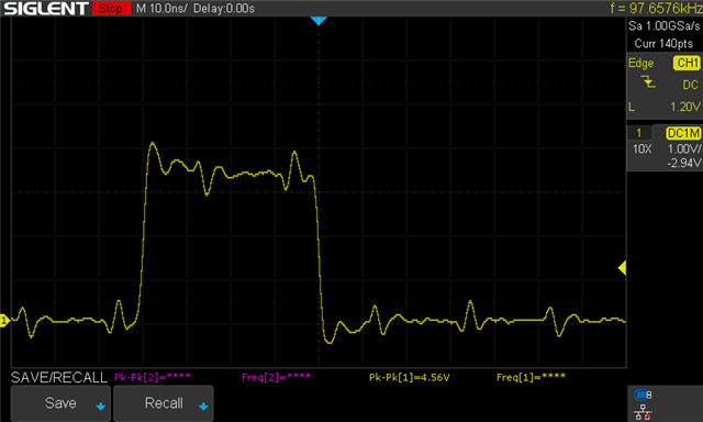
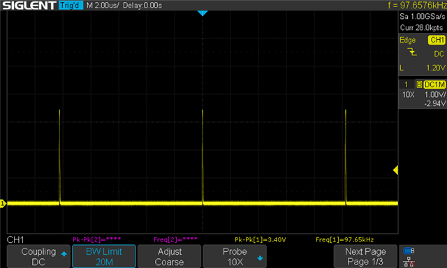
So we're trying to set up the TAA3040 with four differential input channels, DC coupled, and four 32 bit TDM output slots. The chip is slaved to FS and BCLK with internal PLL and all clock setting automatic.

The weird thing is, even if we don't write to the enable bits in IN_CH_EN (they reset to enabled), once the ADC, MICBIAS and PLL are powered up, reading the DEV_STS0 register shows the ADCs powered down, and DEV_STS1 is 6 (Device is in active mode with all ADC or PDM channels turned off).

Question:

Other than waking up the part in SLEEP_CFG being the first event and ADC/MICBIAS/PLL power up in PWR_CFG being the final event, is there a specific order that other I2C registers should be programmed?

What happens if FS and BCLK are running before the chip is configured? Can that prevent correct initialisation?

Thanks

Adam

  • Hi Adam,

    Providing FS and BCLK before the chip is configured is not expected to impact initialization.

    Also, can you provide the list of register configurations being done? From the SLEEP_CFG to ADC/MICBIAS/PLL powerup?

    Thanks and Regards,

    Lakshmi Narasimhan

  • Hey Lakshmi – thanks for getting back to me.

    So it seems that the chip is misreading the FS frequency. We are sampling at a little over 96kHz (it can't be exact due to the PLL settings of the STM32 microcontroller). The ASI_STS correctly reports that he BCLK is 256 x FS, but it reports FS as 768kHz! The error shuts down the ADCs.

    We have, of course, checked that the FS frequency is as expected (and there is a DAC using the same clock signals successfully).

    The order of our initialisation is:

    Wake-up device and select internal AREG in SLEEP_CFG.
    10ms delay
    Set GPIO to HI-Z (as there is an optional MCLK fed to this pin for use without the internal PLL) in GPIO_CFG0

    Set ASI to TDM and 32 bit in ASI_CFG0
    Set a 1 clock delay in ASI_CFG1 for compatibility with the rest of the audio system
    Inputs 1-4 are set to be DC coupled line inputs in CHx_CFG0
    (Optionally enable ADCs 1-4 in IN_CH_EN_ADDR as they are set at reset)
    Enable slots 1-4 in ASI_OUT_CH_EN
    Power-up ADC, MICBIAS and PLL in PWR_CFG
    At this point:
    ASI_STS reports 0x88
    DEV_STS0 reports 0x00
    DEV_STS1 reports 0x60
    So, I guess the first question is what is the tolerance on the 96kHz sample rate (our is actually 97kHz)?
    If we cannot use the PLL, can you please advise settings for using external FS, BCLK and the MCLK driving the GPIO, given FS = 97kHz, BCLK and MCLK= 256 x FS?
    Thanks again Lakshmi – your help is much appreciated.
    Adam
  • Hi Adam,

    I will check and get back on the 96kHz sampling rate tolerance limit.

    In the meantime:

    1) Can you share a scopeshot of the FSYNC waveform at the device pin, do we see any glitches on the FSYNC signal?

    2) Do we see this behavior respond to sampling rate (eg. 48kHz) or BCLK (eg 128*FS instead of 256*FS)?

    Thanks and Regards,

    Lakshmi Narasimhan

  • Hi Lakshmi,

    Here are a couple of 'scope grabs of the FS pin.

    So changing the sample rate to 48kHz with a BCLK ratio at 256 results in the ASI_STS reporting 0x72! Weirder – now it gets the sample rate wrong AND the clock ratio.

    Thanks for your support on this – really appreciated.

    Adam

  • Hi Adam,

    Thank you for sharing the scope captures. The behavior you've mentioned at 48kHz does look weird.

    I have a couple of follow-up questions:

    1) Is this observation found on a single test PCB, or are you seeing this across multiple PCBs?

    2) I see that the IO level for the digital input is 3.3V, does that match with the IOVDD supply as well (Is IOVDD also 3.3V)?

    3) Can you maybe share a PCB schematic of the ADC section?

    Thanks and Regards,

    Lakshmi Narasimhan

  • Hi Lakshmi.

    1) We see this on all 5 prototype boards.

    2) Yes – IOVDD is 3v3.

    We have removed all the checks from the code – so it now ignores the errors, and have disabled ASI bus error checking. ASI_STS still reports 0x88 but the chip actually seems to be working fine.

    So, though the ASI_STS is reporting FS as 768kHz, the TAA3040 has auto-programmed its PLL to the correct 97kHz (ish).

    Could this just be that the FS is not 96kHz exactly and that's confusing the chip?

    Thanks,

    Adam

  • Hi Adam,

    I'll need to set up an EVM and check this out to see if am able to replicate your observations.

    I will do so and update my observations on this thread by the end of this week.

    Thanks and Regards,

    Lakshmi Narasimhan

  • Hi Adam,

    Apologies for the delay. I set up an EVM and ran checks with a sampling rate of 96/97kHz, and a BCLK-to-FSYNC ratio of 256.

    The ASI_STS register was reading 0x58 for this setting, which corresponds to 96kHz sampling rate, and 256 BCLK-to-FSYNC ratio, matching the input clocks.

    As requested before, can you share the schematic/layout for the ADC section in the PCB?

    Also, you mentioned before about "external MCLK driving the GPIO", can you share if you're giving any MCLK to the device, and what is the MCLK frequency?

    Thanks and Regards,

    Lakshmi Narasimhan