This thread has been locked.

If you have a related question, please click the "Ask a related question" button in the top right corner. The newly created question will be automatically linked to this question.

TPA6211A1: Please review the Schematic

Part Number: TPA6211A1

Tool/software:

Hi TIer

Could you help customer review Schematic?

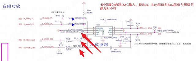
The customer notices that the input resistance preceding the IN+ and IN- is inconsistent with the recommendation in the specification, can this be allowed? 

When using TPA6211A1DGNR audio amplifier, we connect two different audio signal networks (M_VOICE_DAC, S_VOICE2_DAC) at the input negative. This causes the audio gain of each path to not meet the gain of a theoretical calculation. Please help advise if this design is reasonable, here is how resistance matching is calculated to achieve a gain of 4.

  • Hey Yuxi, 

    please follow the application guideline in fig 38. It lays out the best way to apply a schematic with your topology

    Regards,

    Ore.

  • Hi Ore

    As the schematic design shows, the customer has two DACs connected to IN-, which is different from fig 38. I want to check if there is a risk in using this. Also, the customer is using a single-ended model, so we are referring to fig 37.

    May I ask if it is possible to equalize the RI by simply adjusting the resistance values of R212, R215 and R214 in the schematic without altering the circuit ?

  • Rin as in the IC's internal spec? this can't be changed. I strongly suggest sticking to the fig.37 topology then if using single-ended inputs.

    This application is uncommon and may not work. Signal integrity is at risk if there's two analog sources. 

    Regards,

    Ore.