TPA2015D1: Regarding the land size of the components and the NSMD/SMD specifications.

Part Number: TPA2015D1

Tool/software:

Hi team,

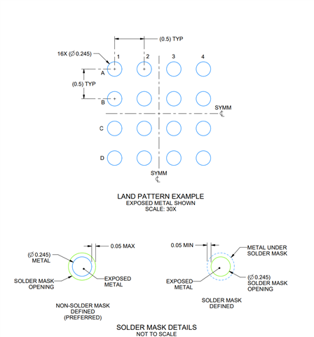
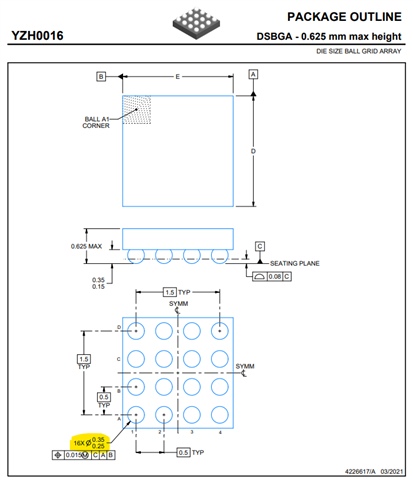
My customer needs documentation that provides information about the pad structure and dimensions—not the solder balls—for the TPA2015D1 during PCB design.

From what I can see on the TPA2015D1 product webpage, the DSBGA package information appears to be fully contained in document YZH0016.

However, it’s unclear whether the circles shown in the bottom view on page 1 of this document represent the solder balls or the component-side lands.


Could you please provide documentation that includes detailed information about the pad structure surrounding the component?

Best regards,

Kyohei

  • Hi Kyohei,

    The content from data sheet page 38 should be usable for the PCB design process. This is the Land Pattern Example.

    Best regards,
    -Ivan Salazar
    Applications Engineer

  • Hi Ivan,

    Thank you for your support.

    I believe the information on page 38 of the datasheet pertains to the metal mask and the PCB side.

    However, what the customer is requesting is the land pattern information for the component side shown on page 37.

    In the upper diagram, does the blue circle indicate the solder ball dimensions?
    And in the lower diagram, is it correct to interpret the light green circle as the land pattern dimensions?

    Best regards,

    Kyohei

  • Hi Kyohei,

    The ball dimension is in previous page:

    The land pattern offers a couple options, in both cases the diameter for the pad is the same 0.245 included in the top LAND PATTERN EXAMPLE figure:

    • Solder mask defined is a bigger portion of metal under the solder mask, the solder mask opening defines the pad dimension.
    • Non-solder mask defined is a bigger hole in the solder mask, leaving some space between the metal pad and the solder mask.

    Best regards,
    -Ivan Salazar
    Applications Engineer