This thread has been locked.

If you have a related question, please click the "Ask a related question" button in the top right corner. The newly created question will be automatically linked to this question.

PCM5242: PCM5242 No Output

Part Number: PCM5242
Other Parts Discussed in Thread: PCM5102A

Tool/software:

Hello, I’ve built a test board for the PCM5242, but there’s no output. Could you help me troubleshoot?

Test parameters are as follows:

  1. Hardware mode with single-ended output
  2. DVDD: 3.3V
  3. External LDO 1.8V by TPS7A2018, which is a bit strange that the measured voltage is 1.88-1.91V
  4. XSMT: Provided 3.3V by MCU IO, powered up 10ms before AVDD, DVDD, LDOO supply
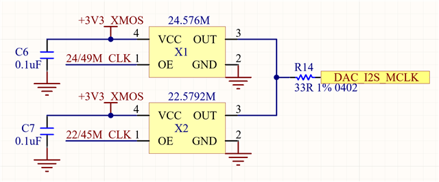
  5. External MCLK from 24.576M/22.5792M crystal, BCK, LRCK, DATA divided from the same crystal by XMOS USB IC
  6. All I2S signals are outputting normally

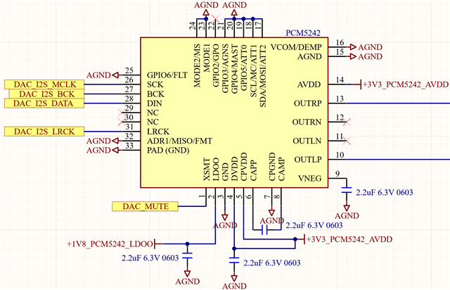
Schematic is as follows

There are no signals at the output at all. VNEG is only 0.47V (I understand it should be -3.3V). After connecting pin 26 (SCK) to GND, there’s still no signal, and VNEG is 0V.

Thank you for your help!

  • Hi Alex, 

    Most problems are coming from incorrect clocks. Based on your schematic, you are setting up your board to be in HW mode with I2S signal. So please probe and plot  all I2S signals on the same screen and make sure it complies with the format that is presented in Figure 19. (I2S Audio Data Format)

    Also make sure your clks values are correct and comply with the below equation, otherwise the part is not gonna give you any output and also the internal CP will fail to function.

    BCLK=  (# of Ch.)   x   (Ch depth)   x   Fs  

    I would put a PU for XSMT to make sure it is not muted when there is no signal on XMST.- You also need dedicated decoupling caps for each external supply ( places as close as possible to the pins). you can use Figure 80. as a reference for their values. 

    Let me know if you still have any issue and I will be glad to help to debug.

    Regards,

    Arash

  • Dear Arash,

    Thank you for your prompt and detailed response.

    1. Regarding the XSMT pin, unfortunately, we cannot hardware-connect XSMT to 3.3V at the moment due to the lack of an exposed pin. We have verified that XSMT is correctly set to 3.3V, and its timing is set to HIGH before the PCM5242 power supplies (AVDD/DVDD/LDOO) are enabled. Even if XSMT were set to HIGH only after I2S transmission starts, shouldn’t the output recover once XSMT is set HIGH?
    2. For the clock signals, we have tried grounding SCK (pin 26) to use the internal PLL, but there is still no output. Could an incorrect clock configuration still cause in this scenario?
    3. The dual crystal oscillators we are using are the standard 24.576MHz and 22.5792MHz, which should meet the requirements specified in Table 32. Could there be other configuration issues we might have overlooked?

    Thank you again for your support. I look forward to your insights.

    Best regards, Alex

  • Hi Alex,

    As long as you verified  XMST is not muting the device ( going LOW) , it is ok.  ( you still need to correct the decoupling caps for supplies later on )

    Have you checked Vneg voltage? is it working correctly? 

    Also let the internal LDO to take over for now

    I would like to see the actual plots of all I2S signals on the same  screen to check the edges . Also the exact value of BCK and LRCLK , as well as the channel depth, is needed to further verify the clks.

    Since it is HW controlled, as long as your format and clks are ok, then it should be straight forward operation.

    Note that the DAC produces diff output for each channel and I  noticed that you connected  as single ended, 

    ( refer to fig 7 in User's Guide) 

    Regards,

    Arash

  • Dear Arash,

    Thank you for your continued support and prompt response.

    We’ve made some progress in testing. I routed the I2S signals to another PCM5102A PCBA, and the audio output worked normally. This confirms that the issue lies with the PCM5242 setup. After comparing the configurations of the PCM5102A and PCM5242, the primary difference is that the PCM5102A uses its internal LDOO, while the PCM5242 is powered with an external 1.8V supply for LDOO. I plan to modify the PCM5242 setup tomorrow to use its internal LDOO for further testing.

    However, I noticed some differences in the power supply configurations between the PCM5242 and PCM5102A datasheets, which raised a few questions:

    1. In the PCM5242 datasheet, DVDD (3.3V) is described as powering the PLL and Oscillator and marked in the red box which indicates analog circuits. However, the name "DVDD" is somewhat confusing, as it suggests a digital supply.
      In contrast, the PCM5102A datasheet shows CPVDD (3.3V) in the red box, powering the Charge Pump and Oscillator, representing analog circuits as well. Does this mean PCM5242’s DVDD is equivalent to PCM5102A’s CPVDD?
    2. If so, what is the role of PCM5242’s CPVDD? Is it solely responsible for the Charge Pump?

    3. If PCM5242’s DVDD is indeed for analog circuits, should AVDD, DVDD, and CPVDD share the same +3V3_AVDD supply?

    Thank you again for your guidance. I look forward to your clarification to help resolve these issues.

    Best regards, Alex

  • Hi Alex,

    These devices are not sharing the same layout or design and the usage of names for DVDD is different in them and a bit confusing.

    For PCM510x while the charge pump has its own dedicated supply ,  PLL was grouped in AVDD supply group  and in the other one, it was powered separately by the supply that was called DVDD. It seems in the diagram for PCM5242 they do not show the charge pump supply. You can power all 3.3V supplies using one source but you have to have dedicated decoupling caps for each supply at the pin location.

    Regards,

    Arash

  • Dear Arash,

    Thank you for your continued support.

    After multiple rounds of debugging, including disconnecting the external 1.8V LDO supply, the situation remains unchanged. I have carefully compared the schematics of the PCM5242 and PCM5102A, and they appear to be very similar with no obvious differences. Could you please review them again to check for any potential errors we might have missed? I’ve attached the schematics for your reference.

    At this stage, I am considering the following possible causes:

    1. Pin 22 is currently floating. Should it be connected to GND? Could this affect the PCM5242’s operation?
    2. The outputs OUTRN and OUTLN are floating. I recall confirming earlier that these pins should be left floating if balanced output is not required, but could this still have an impact?

    Thank you again for your assistance. I look forward to your guidance on these points.

    Best regards,

    Alex

  • Hi Alex,

    I don't see any difference b/w the 2 schematics that make a complete fail.  

    Since you are using the device in HW mode, pin 22 is an output and should be left alone. In SW mode it makes a difference to connect it to GND or not. 

    You can leave the unused outputs float as well. 

    If you have checked all supplies at the pin and they are all correct, (since you are sending a verified I2S signal set to the chip) then it might be the chip has been damaged or has a problem itself.

    Devices in HW mode-once they have correct supplies and I2S - they should work fine.

    I would suggest to replace the part to be sure, if still the problem exists, then it would be your board itself. 

    Regards,

    Arash

  • Dear Arash,

    Thank you for your guidance and support. We understand the situation and will proceed with fabricating a new PCB for further testing.

    Thank you again for your assistance.

    Best regards,

    Alex