This thread has been locked.

If you have a related question, please click the "Ask a related question" button in the top right corner. The newly created question will be automatically linked to this question.

NE5532: NE5532P Datasheet Version Differences & Internal Diagram Inquiry

Part Number: NE5532

Dear TI in charge,


With reference to the NE5532P, our FAE has reviewed the available datasheets and noted that there are multiple versions published in 2004, 2009, and 2025.

The 2004 and 2009 versions show the same full internal diagram, while the 2025 version presents a simplified internal diagram.

Based on this difference, we would like to check whether TI has made any specification or internal design changes to the NE5532P. Additionally, could you please share the full internal diagram of this IC again?

The customer is concerned that certain internal transistors or diodes at the input (+/–) stage may have been removed, as this could impact the device’s operating characteristics and their circuit design.

Thank you,

Sirion


  • Dear TI incharge.

    Sorry, the correct forum is Amplifier, FYI.

    Thank you,

    Sirion

  • Hi Sirion,

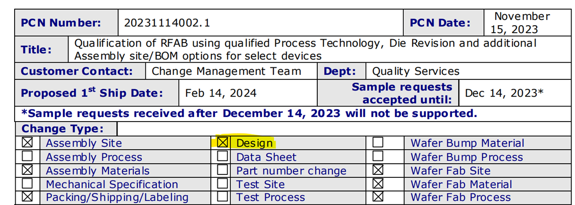
    The 2025 datasheet reflects the design and assembly updates to the NE5532P, the details of which can be found in this PCN here. I cannot provide the internal design layout of the NE5532P, but the internal ESD protection has been updated. Both the inverting and non-inverting inputs have ESD protection to the positive supply, and the output pin has ESD protection to each supply.

    Best regards,
    Carrie

  • Dear Carrie,

    Thanks for your reply.

    It is fine if the internal design layout cannot be shared.
    We also note that the ESD protection circuit has been added to the I/O pins.

    However, we would like to confirm one key point:
    Do the two transistors (marked in red in the link below) still exist in the latest 2025 specification revision?

    We would appreciate it if TI could kindly confirm this.

    https://www.dropbox.com/scl/fi/iqa8avb3j1g7x8e0it3cr/NE5532_Input-Transistors.jpg?rlkey=0p3zyizj8fpd3i4s4v2rzbwp1&dl=0 

    Best regards,
    Sirion

  • Hi Sirion,

    Can you please upload the photo directly? I cannot see the photo you are referring to from the current link.

    Best regards,
    Carrie

  • Hello Carrie,

    Pls refer to the image in the Excel file.

    Do the two transistors (marked in red) still exist in the latest 2025 specification revision?

    Pls clarify.

    Thank you,

    Sirion


    NE5532P.xlsx

  • Hi Sirion,

    The two transistors do not exist in the 2025 version. The inputs have ESD protection to the supplies, not between inputs. 

    Best regards,
    Carrie

  • Hi Carrie,

    Could you please provide a PCN or official documentation that confirms the removal of the two transistors?

    Our customer requires formal documentation to verify this specification change.

    Also, regarding the PCN you mentioned earlier, could you point out which page or section specifies the details of the ESD protection update?

    Thank you very much,

    Sirion

    PCN20231114002.1.pdf

  • Hi Sirion,

    The PCN shows that the design was updated, as you can see from the below screenshot. We do not share the specific changes of the device design for proprietary reasons. Please note that the updated ESD structure does not affect the device during normal operation. For more information on ESD updates in new devices, please see Section 6 of this app note.

    Best,
    Carrie

  • Hi Carrie,

    Thanks for the clarification.

    We understand that the detailed design changes can’t be shared.
    In this case, could you advise how the customer should handle any necessary circuit changes to use this device without issues?

    Are there any general design guidelines, recommended external components, or layout considerations related to the updated ESD structure that customers should follow?

    Any high-level guidance would be very helpful.

    Thanks for your support.

    Best regards,
    Sirion

    Electronics Source Co., Ltd.

  • Hi Sirion,

    The customer should not need to make any changes to design or layout. The ESD cells are designed to only operate when they sense an electrical overstress event, so the device will act as expected when in linear operation. If the customer does in circuit tests before operation, they will likely have to adjust their limits. This is due to the  "diode curve" of the ESD cells being different than before. Otherwise, there should be no need for schematic or layout changes.

    Best regards,
    Carrie