This thread has been locked.

If you have a related question, please click the "Ask a related question" button in the top right corner. The newly created question will be automatically linked to this question.

TLV320AIC3104: Auido leakage issue

Part Number: TLV320AIC3104
Other Parts Discussed in Thread: TS12A12511, PGA2311, TPA6120A2, OPA1612, OPA1622,

I am experiencing audio crosstalk on my audio driver PCB and would appreciate some help identifying the source.

Signal chain:

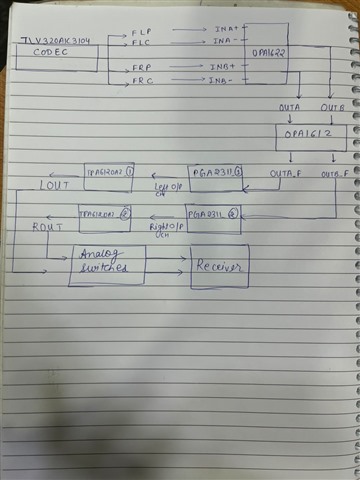
MCU (I2S/I2C) → TLV320AIC3104 → OPA1622 (buffer) → OPA1612 (Sallen-Key filter) → PGA2311 volume controls → TPA6120A2 → TS12A12511 analog switches → receiver outputs.

The board has two audio paths: Tone and Masking.

Problem:
When both analog switches are enabled at the same time, I can hear the Tone signal on the Masking output. The issue is most noticeable when the masking volume is set to a very low level. The leaked tone is clearly audible.

PCB details:

  • Split ground plane used.

  • TLV320AIC3104 located on the left side.

  • PGA2311 located on the bottom-left side.

  • TPA6120A2 located on the top-right side.

  • Analog switches and mono jack connectors located on the bottom-right side.

  • Ground planes are connected through a 0-ohm resistor.

  • I have also tried adding multiple ground stitching vias between the ground sections, but the leakage is still present.

Questions:

  1. Could the split ground arrangement or ground return paths be responsible?

  2. What measurements should I make to determine which stage is introducing the crosstalk?

** 3D view of my PCB is attaached 
**Note that the board layout is of 2 layers 
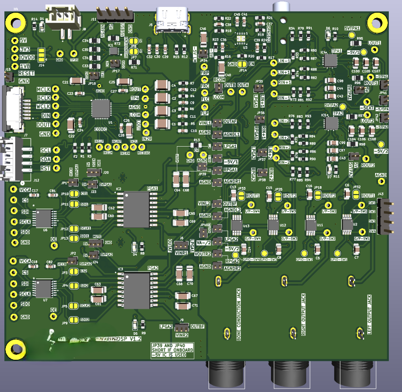


Screenshot 2026-06-08 171532.png

  • Hi Falguni,

    There are a lot of stages between the codec and the receiver outputs. Have you probed to see where the leakage starts or how far back up the chain it is?

    Would you be able to provide a schematic as well so I can see how the codec is connected to the two output paths?

    Thank you,
    Jeff McPherson

  • Thank you for your response.

    I am not able to clearly observe the leakage on my oscilloscope. Even when I reduce the vertical scale to 1 mV/div, I do not see a noticeable sine wave on the receiver output where the leakage is heard.

    The leakage is only audible under the following condition:

    • A tone is being played on the left channel.

    • The right channel output path is also enabled.

    • The masking volume on the right channel is set to a low level.

    In this situation, I can clearly hear the tone signal leaking into the right receiver output, but I am unable to capture a corresponding waveform on the oscilloscope.

    Could this indicate that the leakage level is extremely small but still audible through the receiver, or is there a better measurement technique you would recommend for identifying the source of the crosstalk?

    In the meantime, I have a question regarding PCB grounding practices for mixed-signal audio designs. My signal chain includes the TLV320AIC3104 codec, PGA2311 volume controls, TPA6120A2 amplifier, analog switches, and digital interfaces such as I2S, I2C, and SPI.

    For this design, I used split ground planes, with the analog and digital sections separated and connected through a 0 Ω resistor. I also tried adding ground stitching between the planes, but the leakage issue remains.

    I noticed that the PGA2311 datasheet recommends separating analog and digital grounds around the device. However, I often see recommendations for using a single continuous ground plane in modern mixed-signal designs.

    For future revisions, what would be considered the best practice for a design like this?

    • A single solid ground plane for the entire board?
    • Separate analog and digital ground planes connected at one point?
    • A single ground plane with careful component placement and return-current management?

    I would appreciate your guidance on the recommended grounding approach for minimizing audio crosstalk and noise in this type of mixed-signal audio design.

    Thank you,
    Falguni

  • Hi Falguni,

    If you can't see it on a scope, is it possible to control which stage is active between the left and right sides? For example, you leave the left channel in normal operation, and then you mute the right channel at each device going backwards up the chain. You mention that the right channel is enabled but playing a very low volume so I wonder which device the crosstalk is coming from.

    If the crosstalk is not very loud it could be difficult to see the sinewave on a typical scope. If you have any kind of FFT function on the scope or someway to measure the frequency domain, that might give more insight into how the crosstalk is performing.

    If you could also send me your I2C configuration script I can check on my EVM to see if the leak is happening at the device, since you mentioned you've already taken a lot of steps at controlling the layout. I have seen in the past leakage issues happening based on the order in which the registers are written to. I'm not sure that's what's happening here but I could still check it if I have your I2C configuration. Order matters so I would need a script, not a register dump.

    Regarding the ground planes, I would go with split analog and digital planes by default. Audio is a very sensitive application so it is usually worth the effort to keep digital noise away from the analog signals. However you can achieve the same by carefully managing the return currents for the supplies and analog signals i.e. your third option. This is of course dependent on each device and their own requirements but that's my general rule of thumb.

    Best regards,
    Jeff McPherson

  • Hi Jeff,

    Thank you for the detailed response.

    Regarding the TLV320AIC3104 configuration, below is the register write sequence that I am currently using. Could you please let me know if this initialization sequence looks correct, or if there are any registers that could potentially contribute to channel leakage or crosstalk?

    tlv_write_reg(i2c_dev, 0, 2, 0b00000000); // 0
    tlv_write_reg(i2c_dev, 0, 7, 0b01101010); // 106
    tlv_write_reg(i2c_dev, 0, 3, 0b10010001); // 145
    tlv_write_reg(i2c_dev, 0, 4, 0b01000000); // 64
    tlv_write_reg(i2c_dev, 0, 11, 0b00000001); // 1
    tlv_write_reg(i2c_dev, 0, 5, 0b00000000); // 0
    tlv_write_reg(i2c_dev, 0, 6, 0b00000000); // 0
    tlv_write_reg(i2c_dev, 0, 101, 0b00000000); // 0
    tlv_write_reg(i2c_dev, 0, 102, 0b10100010); // 162
    tlv_write_reg(i2c_dev, 0, 8, 0b00000000); // 0
    tlv_write_reg(i2c_dev, 0, 9, 0b00110000); // 48
    tlv_write_reg(i2c_dev, 0, 10, 0b00000000);
    k_msleep(10); // 0
    tlv_write_reg(i2c_dev, 0, 41, 0b00000010); // 2
    tlv_write_reg(i2c_dev, 0, 43, 0b00000000);
    k_msleep(10); // 0
    tlv_write_reg(i2c_dev, 0, 37, 0b11010000); // 208
    tlv_write_reg(i2c_dev, 0, 38, 0b00001000);
    k_msleep(10); // 32 
    tlv_write_reg(i2c_dev, 0, 64, 0b10000000); // 128
    tlv_write_reg(i2c_dev, 0, 47, 0b10000000); // 128
    k_msleep(10);
    tlv_write_reg(i2c_dev, 0, 51, 0b00001101); // 13
    tlv_write_reg(i2c_dev, 0, 65, 0b00001101); // 13

    I also have a question regarding the grounding strategy.

    My board uses separate analog and digital ground regions connected through a 0 Ω resistor. After adding ground stitching vias between the ground regions, I noticed a significant improvement in the crosstalk issue. This makes me think that return-current paths and grounding implementation may be playing a role in the behavior I am seeing.

    For future revisions, if I continue using split analog and digital grounds, what would be the recommended implementation on a 4-layer PCB?

    For example:

    • Should one internal layer be dedicated to analog ground and another to digital ground?

    • Should audio signals be allowed to cross between the analog and digital sections?

    • If signals must cross the split boundary, what is the recommended routing practice and return-current strategy?

    • Is a single-point connection preferred, or should stitching vias be used along the boundary between the analog and digital sections?

    I would like to understand the recommended layout approach for mixed-signal audio designs using devices such as the TLV320AIC3104, PGA2311, and TPA6120A2 so that I can apply the correct grounding strategy in future designs.

    Thank you for your guidance.

    Best regards,
    Falguni

  • Hi Falguni,

    The datasheet has a layout guide but it's hard to see the ground split. I have made a drawing of it below.

    You should do something like the following

    Top Layer - Signal layer with split ground

    Middle Layer 1 - Ground Plane with split ground

    Middle Layer 2 - Power Plane

    Bottom Layer - Signal Layer with split ground

    I think keeping the grounds separate on each layer will prevent any accidental signal crossing. You should minimize any signals crossing the boundary and if they do, you should take care that their return path doesn't intersect another path from the other plane (digital to analog or vice versa).

    A small amount of net ties (2-3) should be enough to join them together. Try to do this away from the device.

    Best regards,
    Jeff McPherson

  • Hi Jeff,

    Thank you for the clarification regarding the grounding strategy.

    I have a few follow-up questions:

    1. Could you please comment on the TLV320AIC3104 initialization sequence that I shared earlier? Does the register write order look correct, or do you see anything that could potentially contribute to channel leakage or crosstalk?
    2. Regarding the AGND-DGND connection, is there any practical difference between using a 0 Ω resistor and a net tie for joining the ground regions? I understand both provide a connection between the grounds, but I would like to know if one approach is preferred over the other for mixed-signal audio designs.
    3. For future revisions, should I partition the ground pours on inner layer1  into separate analog and digital regions as shown in your example.
    4. In my design, the codec is located between the digital MCU section and the analog audio chain. Is it acceptable for the ground split boundary to pass through the middle of the board near the codec, effectively separating the digital and analog sections, or would you recommend a different partitioning approach?

    I would appreciate any additional guidance on how you would implement the AGND/DGND partitioning for a mixed-signal audio design using the TLV320AIC3104, PGA2311, and TPA6120A2.

    Thank you for your help.

    Best regards,
    Falguni

  • Hi Falguni,

    Jeff is out of office, please give us some time to respond to this thread.

    Best,

    Garret