PCM1789: ATTENUATOR REGISTER

Part Number: PCM1789

VOLUME CONTROL FUNCTION 

WHAT WOULD PREVENT VOLUME FROM CHANGING WHEN THE CONTENT OF REGISTERS 24 AND 25 ARE ALTERED. MY OUTPUT LEVEL IS APPROX 75 mVPP. THE APPLICATION USES I2C FOR CONTROL.

REGISTER CONTENTS C0 00 00 00 00 03 00 00 FF FF

WHAT ARE THE LOGICAL REQUIREMENTS FOR THE VOLUME CHANGES TO TAKE EFFECT?  LKCLK IS 48 KHZ CHANNELS ARE 32BIT.

ANY SUGGESTIONS?


THANKS

  • Hello Jerry,

    This device has a very simple register set and seems most of your registers are set as default or normal operation;I don't see any issue with them.

    Here are few suggestions to check or consider:

    • For FF in registers 24 and 25 you don't have any attenuation but if you set it to attenuate, the changes in attenuator levels are made by incrementing or decrementing one step  for every 8/fs time interval until the programmed attenuator setting is reached. So for 48KHz, it takes   ( t= 16.66us  * # of steps)  to reach the final target attenuation. 
    • Also note based on Table 11. beyond a value for attenuation, the attenuation is already reaching the mute level.

    Aside from the attenuator, 

    • the full differential output voltage is 8 Vp-p , if you are sending a full scale or anything close to that, then  vout of 75mV that you are getting is very low. I suggest you verify  that you are getting the full expected Vout for a FS input first , if not , you have a different issue and  the DAC is not doing the digital to analog conversion to begin with! 
    • Check your clks , they have to adhere to the following relationship:

                 BCLK= # of Ch.  *  Ch depth  * Fs          ===> so your BCK has to be 2x32x48kHz for the above specs you mentioned.

    • Also make sure your format matches exactly with the corresponding figure in page 20. Table 4 also needs to be verified. Format mismatch  will  cause the dac to malfunction.

    Kind Regards,

    Arash

  • Hello Arash,

    Thanks for your help. I find the datasheet wave forms have transitions of LRCK coincident with the rising edge of BCLK. The data sheet shows the falling edge of BCLK coincident with LRCK. I am running both the data source and the DAC in slave mode with a 12.288MHz crystal oscillator and an eight bit synchronous counter deriving BCLK from Q2 and LRCK from Q8. This provides rising edges of BCLK and LRCK to be coincident. Can this interfere with the frame count employed in changing atenuator settings not changing?

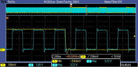
    i have attached a scope data picture showing BCLK in blue and SDATA in yellow. the rising edges are all within the logic state of SDATA. I have also a screen shot of the 24 bit I2S waveform from the data sheet.

    J  erry 


  • Hello Jerry,

    If you used a 1KHz sinewave input at FS and  the output is not a FS sinewave at 1KHz (The full-scale output voltage is (1.6 × VCC1) VP-P in differential output mode) , then most probably it is the I2S input issue. 

    •   Please first confirm you are using Fs=48K, 32b, BCK=3.072M, MCK=12.28MHz.
    •  Then to debug the I2S format validity,  plot BCK , LRCLK and Din (preferably on separate axis  as shown in figure 30). 

    I want to see the start of a channel where the MSB starts ( the rising edge of first data with respect to BCK and LRCLK position) . With I2S format ,  each channel starts with LRCLK edges where  BCK is falling at either edge of LRCLK and the Data comes with ONE BCK delay,  at BCK falling edge.

    I have used this device without programming any registers and it just works fine with simple power up. So the issue most probably is the format of your I2S  is not what device is expecting or the value of clks are not as I indicated above.

    Regards,

    Arash

  • Confession time.... I am confused. From the datasheet, I made an assumption that 0xffff was the most positive I2S code, 0x8000 was the no signal value or zero value, and that 0x0000 is the most negative value. This is the scheme employed to convert .wav signed 2's complement values to the I2S serial data. In the n'th review of the data sheet, i read a statement that the negative values must be 2's complement. Can you point me to a definition or spec that defines the I2S data stream for simple folks.  My requirement for now is to use 16 bit data but would like to keep the option to use 24 bit samples.

    i thank you for your help

    Jerry

  • The popular I2S ASI formatted data is transmitted as a binary two's complement . For converting a number to its negative value, you simply invert  all the bits and then add 1.     

    for example

    25 is   0001 1001

    -25 is  1110 0111

    There are many videos on youtube or pages   like this (link) that you can refer.

    Regards,

    Arash