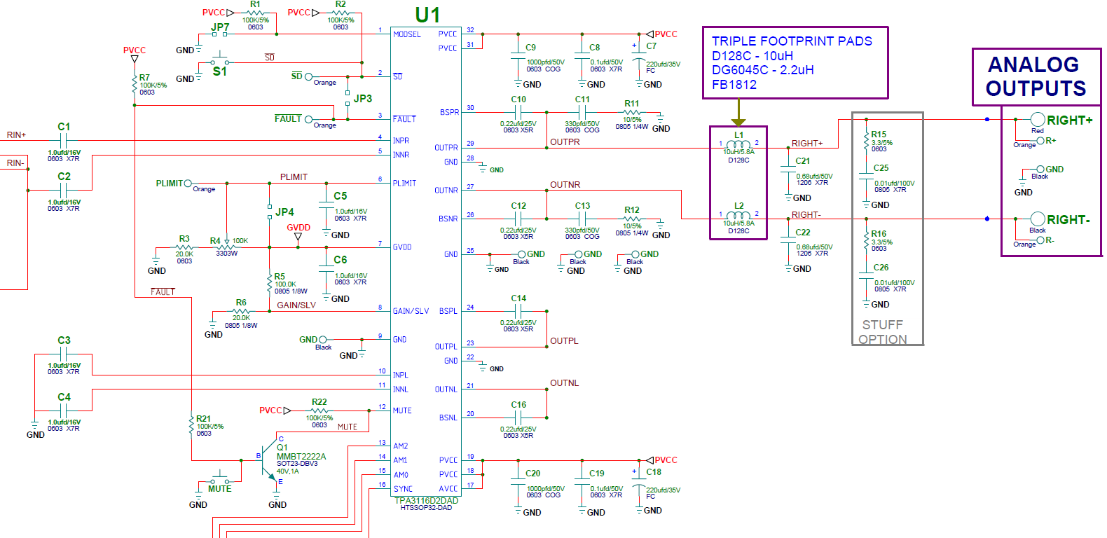
This thread has been locked.

If you have a related question, please click the "Ask a related question" button in the top right corner. The newly created question will be automatically linked to this question.

TPA3130D2 SDZ & MUTE

Other Parts Discussed in Thread: TPA3130D2, TPA3116D2, TPA3130D2EVM

Dear, Sir.


We are promoting TPA3130D2 for a audio system, analog input and Mono 4ohm/20W output.

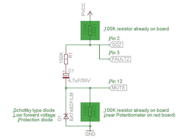
The customer faced pop noise problem before, hence serious for mute function.

TPA3130D2 has 2 pins, SDZ & MUTE to be used for mute fuction(turn off output transisters).

These are his questions regarding those 2 pins to consider which is the best to realize the

mute function.

1. SDZ looks like to be able to clear protection latch.

    Will other setting such as Gain setting be cleared due to SDZ pin low (like reset)?

2. I wonder MUTE will be simply turn off output transisors keeping all setting.

   Correct?

3. Page 6 on the data sheet, defines ton/toff.

   Can these parameters be referred for MUTE?

4. SDZ will be the best during power off/on stage.

   Which is the best way to realize mute fuction(set no output, normal operation stage), SDZ or MUTE?


Hoping to get your advices.

Best Regards,

  • Someone help me!!

    Best Regards, 

  • Sakai-san

    both SDz and MUTE can be used.

    MUTE set the output OFF while keeping the internal circuitry running, so it has a faster start, but will also draw more idle current.

    SDz stops the complete device bringing it in shutdown state, with minimum idle current.

    so what to choose depends on the application - for battery operation chose the SDz, else choose the MUTE function.

    rgds,

    Kim Nordtorp Madsen

  • Dear, Kim-san. 

    Thank you your  valuable and helpful teachings. 

    Sorry again, but I would like to ask another. 

    Page12 & 13 on the data sheet, Supply voltage vs. Max Output Power characteristics chart

    are described on(RL=2 & 3ohms). 

    I wonder you had a similar chart, case of RL=4ohm? Please send it to me. 

    If you don't have, calculation formula for it will be also helpful for me. 

    Best Regards, 

  • Sakai-san

    you can use BTL 4R load case to see output power, page 7-8

    rgds,

    Kim 

  • Dear, Kim-san. 

    Do you mean all characteristics of BTL case can be referred to PBTL? 

    Sorry, again and again. 

    Best Regards, 

  • Sakai-san,

    PBTL parallels the two output H-bridges, and allows you to get slightly closer to the rail. So, the power will be a little bit more in PBTL mode than BTL mode, but looking at the BTL data will give you a good idea of what to expect in PBTL.

    I am not sure why you would want to use 4R PBTL. The part can easily handle 4R BTL.

    -d2

  • Dear, Don-san. 

    Thank you for your valuable advice. 

    I just know the customer want to apply MONO MODE, it is the reason why selected PBTL

    following datasheet. 

    Best Regards, 

  • Hello, Sakai-san. I can see why you would want to use PBTL after looking at the Mono Mode section of the data sheet. Fortunately, you can use BTL instead of PBTL to drive a 4 Ω load, so you'll need fewer components to achieve the results you want. I've come up with two adapted schematics to show you how to do this, one of them I prefer.

    This first schematic assumes you are using a single channel of audio input. In this case, we can remove the snubbers at the left switching output. I prefer this design, because with no left audio input, there isn't a left switching output, and the chip does not need to work as much.

    This second schematic assumes you use a left and right input into your audio system. The left audio channel will not appear at the speaker (because only the right channel will reach the speaker in this schematic; see the TPA3116D2 block diagram in the data sheet for details), but the schematic has all the components you would need to route the left audio to a switching output, and not have it go to a speaker.

    Best Regards,
    Matt

  • Dear, Matt-san. 

    Thank you for your detail information. 

    We delivered TPA3130D2EVM to the customer and they started the evaluation 

    Unfortunately, they are facing one trouble about  too much PVCC current(0.42A@

    Pvcc=12V). It observed just to supply PVcc under no load.

    1. According SLOU341(User's Manual), EVM version looks "B". But the version of

        delivered EVM is "C".   "C" looks little bit different from "B" 

        Could you provide The schematic of version"C"?

    2. They are evaluating with the jumper setting as original(no change from EVM delivery). 

        Could you clarify the correct jumper setting? 

        JP1, JP2, JP3, JP4, AM0, AM1,AM2. 

    PS) For PBTL mode, INPL & INNL should be connected to GND immdiately. Just use RIN only. Right? 

    Best Regards, 


  • Hello, Sakai-san. That is more power supply current than I would expect for not having a load, but it isn't outrageously larger than I would expect.

    To answer your questions:

    1. The "C" version of the TPA3130D2 EVM is different from the "B" version. I have attached its schematic below this sentence. I am sorry that it wasn't available in the User's Guide. I am working to fix this.
      8562.TPA3130D2 EVM Schematic Rev C.pdf
    2. The following headers require shunts across them: AM0, AM1, AM2, JP1, JP2, JP3, JP4, and MODSEL. 

    For PBTL mode, yes, use RIN only. I recommend connecting INPL and INNL to GND through a capacitor, as I have shown on my example schematics in my previous post. I assume they are not routing audio into INPL and INNL. Can you please confirm? Note that the TPA3130D2 EVM does not have the headers that allow a shunt to GND, as the TPA3116D2 EVM does, so it will take some more work to connect the left inputs to ground on the EVM.

    Best Regards,
    Matt

  • Hallo Dear Matt

    I'm waiting your samples of the TPA3116, to realize a new ClassD Amp for Italy market. In the meantime I'm studing the Pcb. I've some doubts about the MODE pin configuration. In all diagrams you have a switch, indicating MUTE, but in the real application I haven't any switch ! How to command the Mute pin ??

    waiting for your kind reply I remain..

    thank you in advance

    Frank

    MITHOS ITALY

  • Hello Frank,

    We're glad to hear you're using TPA3116 for this new application! 

    What are you referring to when you say "the real application"? On the EVM / PCB, the MUTE pin is triggered by a fault condition, or by a switch, as you said. You need some way to bring it low if you want to mute. I'm not sure I understand your question...

    Best regards,
    Arnold Zhang 

  • Hello Arnold

    as "real application" I intend that in the customer PCB they don't have any switch, the Mute must be automatic when they switch-on the amp, right?

    I know that I must control the Mute pin , only I fear to have pop-noise in the speaker, when switch on or switch off ! How to avoid any pop noise?

    Maybe a capacitor as soft-start it's enough?

    Pls suggest a schematic for the MUTE control...without switch!

    thanks in advance

    Frank

    MITHOS ITALY

  • Hey Guys, im trying to figure out a power-on speaker bump solution as well. How would I add a short delay to avoid the speaker bump? Using the mute pin or sdz?
  • This is a circuit that I have designed and successfully implemented onto a Yuan Jing Audio amplifier based on TPA3116D2 , to prevent pop noise when turning on:

    At power-on (21V) this circuit holds to high logical level MUTE pin for about 2 seconds. This delay is shorter at lower operating voltages, but it is enough to avoid any bump (tested from 7 to 26V).

    The delay can be adjusted by changing the values of C1.

    Wait a few seconds after shutting down the amplifier before turning it back on again, to allow power supply capacitors and C1 to discharge, otherwise it is possible to hear a bump.

    This circuit cannot prevent popping noise at power off. In such a case a circuit to detect that AC mains voltage has been switched off is needed. It could be done, for example, with an optocoupler and a voltage comparator.

    The only concern was about the negative voltage on MUTE pin  that is present during power-off transient period, due to discharge of capacitor C1.

    For TPA3116D2 the absolute negative limit voltage on MUTE input is only -0.3V!! (see datasheet).

    The problem has been solved with a protection schottky diode D1 across MUTE pin and gnd .

    Use only a small signal schottky diode type, like a BAT48 diode, as indicated in the schematic, that will clamp voltage on MUTE pin within the maximum absolute value.

    DO NOT use silicon diodes!

    Resistor R1, and upper 100K smd,  limit discharge current to less than 0.1mA.

    At 0.1mA (Tj = 25° C) BAT48 has a maximum forward voltage drop of only 0.25V and it is well suited for the scope.

    1PS76SB40 diode (package=SOD323,  marking code S4)  is also a good choice. I've mounted it on top of smd resitor (see photo below).

    Note: I've connected R1 to an smd resitor (100K) connected to SDZ/FAULTZ and PVCC on the other side, only for convenience, because it is easy to implement on my board.

    This connection does not interfere with the proper operation of the amplifier, anyways it is possible to connect R1 directly to PVCC. In such a case increase R1 value to 220K.

    Any comment/suggestion is welcome!

    Giancarlo

    Bologna, ITALY